📝 29 Aug 2021
UPDATE: There’s a new version of PineDio Stack BL604, the GPIO Numbers have changed
What’s it like to create Open Source Software (and firmware) for brand new Prototype Hardware?
What interesting challenges will we encounter?
Find out how we create new firmware to test (and improve) Pine64’s newest and hottest prototype: PineDio Stack BL604 RISC-V Board!
⚠️ Obligatory Disclaimer: Features included in The Prototype are not complete, and will most certainly undergo changes before becoming available for public consumption. (Burp) They are described here for testing, exploration, education and entertainment purposes only. The Prototype shall NOT be used in production gadgets. (Like toasters, microwave ovens, and most definitely not, pressure cookers)
The kind (and super cool) folks at Pine64 told me that I would be receiving a fun new gadget that’s…
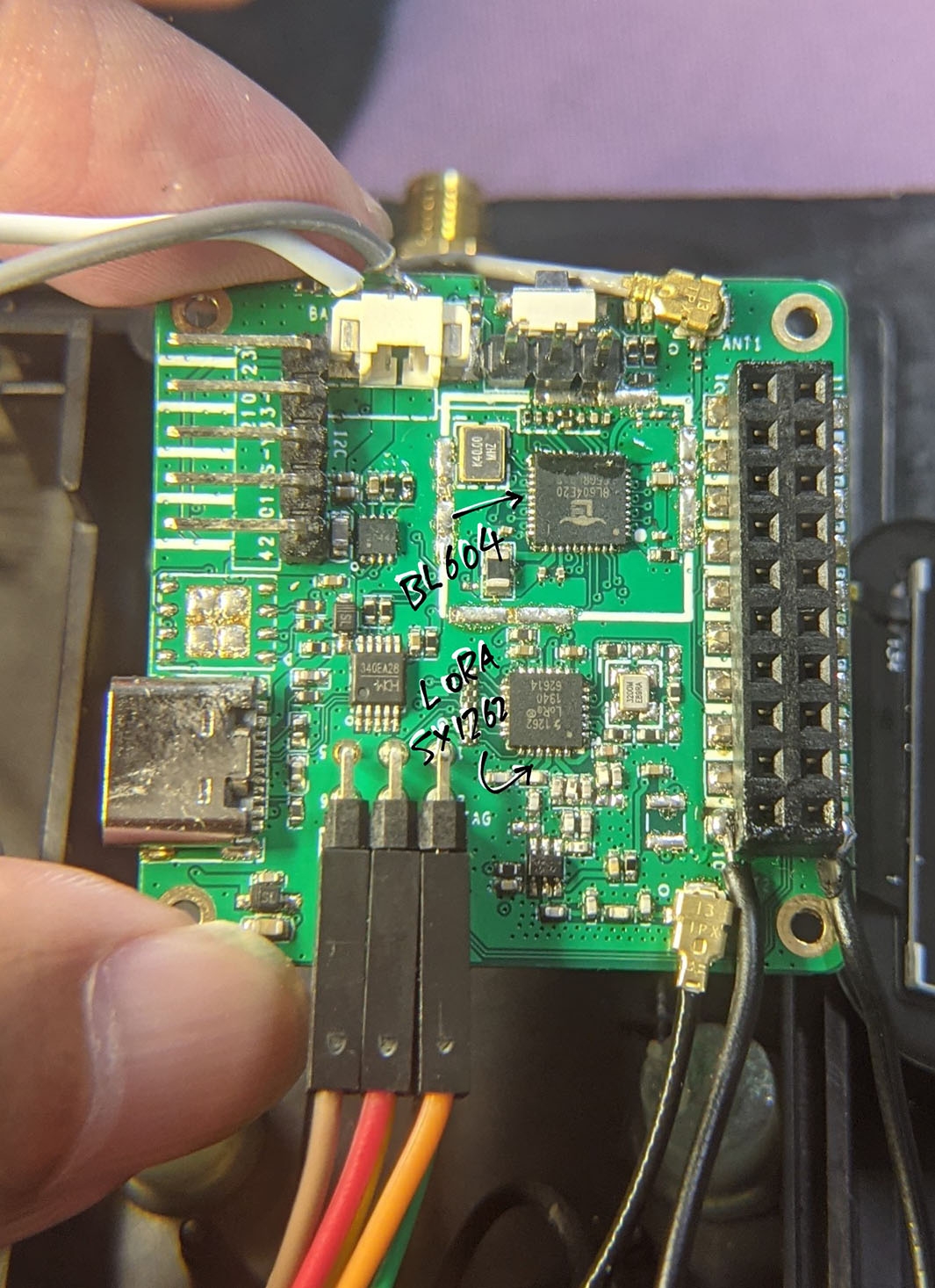
Based on BL604 RISC-V + WiFi + Bluetooth LE SoC, which is the upsized sibling of Bouffalo Lab’s BL602 SoC.
(BL604 has 23 GPIOs vs BL602’s 16 GPIOs. So it’s like comparing millipedes and centipedes, I guess)
And BL604 is supposed to be 100% compatible with BL602
(Is it really 100% compatible? We’ll find out in a while!)
Has an ST7789 SPI Display
(Imagine the possibilities)
Has an onboard LoRa SX1262 Transceiver for low-power, long-range, low-bandwidth networking
(Wow!)
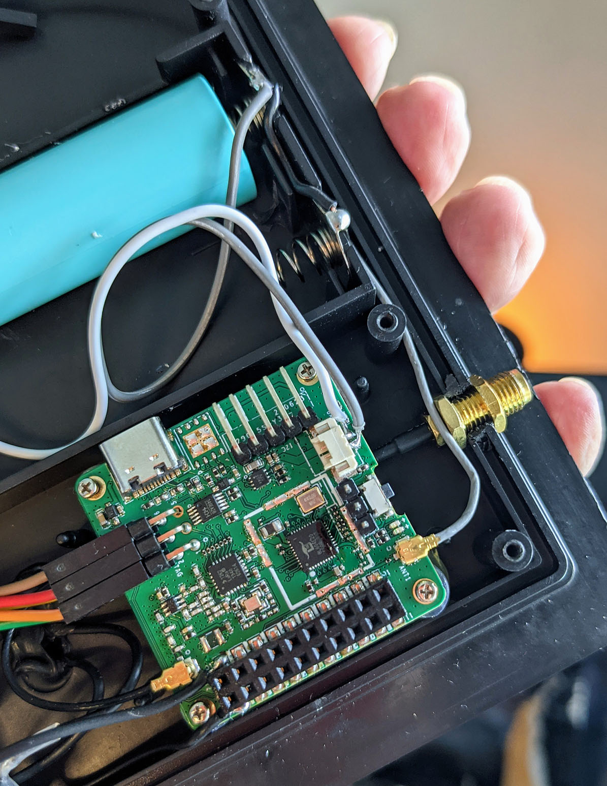
Plus SPI Flash, Battery Charging Chip, Accelerometer (optional) and Heart Rate Sensor (optional)!
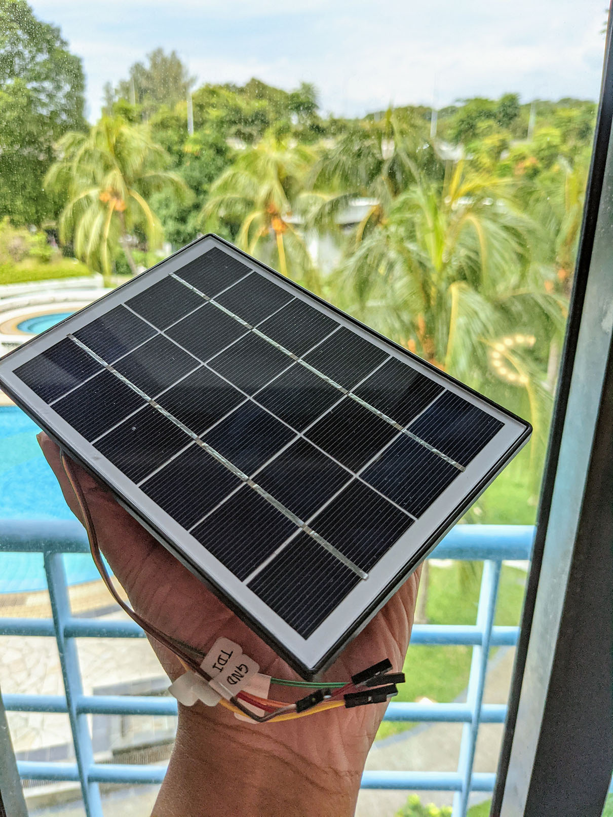
After some shipping delays at Shenzhen (due to flooding or pandemic?) I received something totally unexpected…
A Solar Panel!
(Yeah Singapore is super sunny… Is this mockery? 🤔)
But a Solar Panel with a JTAG Cable? That’s highly unusual.
Opening the gadget reveals the hidden treasure inside: PineDio Stack BL604 Board!
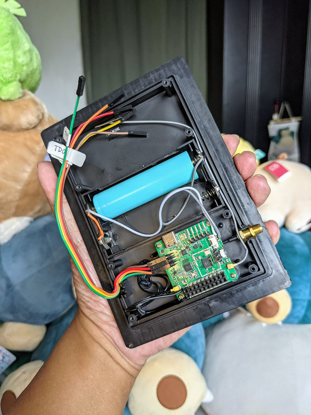
That’s typical of Prototype Hardware fresh from the factory: No docs, no fancy packaging, no branding either.
(Ground Plane is also missing, which we’ll fix before FCC Certification)
We shall explore PineDio Stack ourselves… And document all our findings for the sake of the Open Source Community!
What’s on the underside of PineDio Stack?
Unscrewing the board (from the glue sticks?) reveals the LCD Display Connector on the underside of the board…
The connector matches this familiar ST7789 SPI Display that was shipped with PineDio Stack…
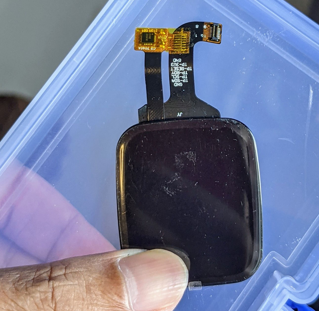
So we snapped the ST7789 Display to the board…
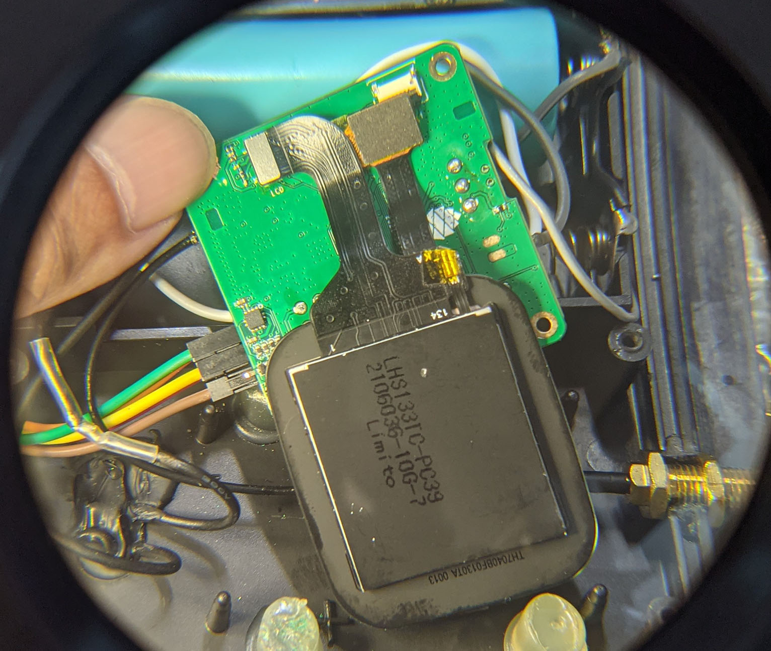
And we get an unusual contraption: A Solar Panel with LCD Display inside!
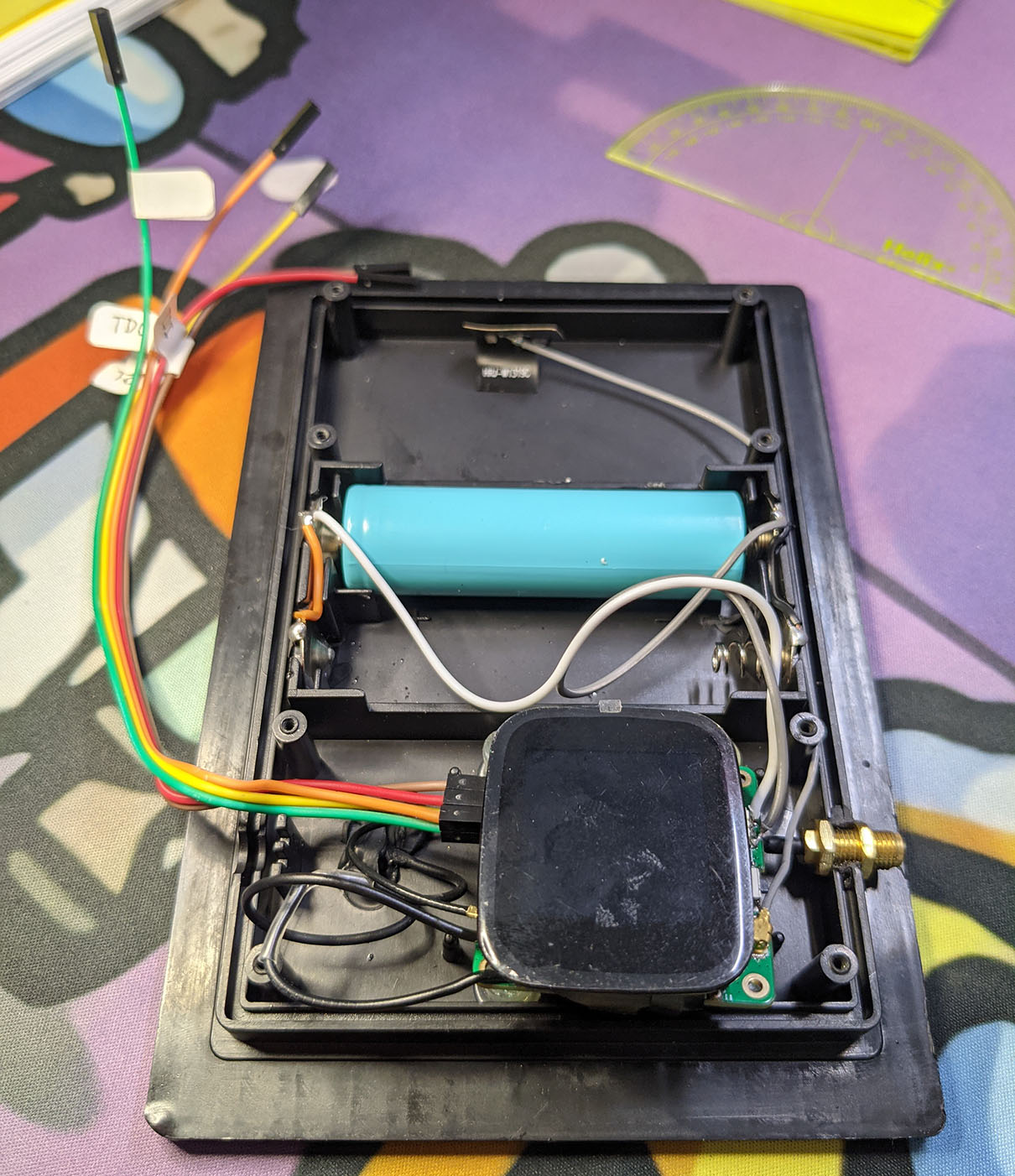
We’re ready to test our firmware on PineDio Stack! We’ll follow this schematic…
What’s the first thing that we run on a brand new prototype board?
Blinky Firmware of course! (Yep the firmware that blinks the LED)
/// PineDio Stack LCD Backlight is connected on GPIO 21
#define LED_GPIO 21

/// Blink the LED
void blinky(char *buf, int len, int argc, char **argv) {
  //  Show a message on the serial console
  puts("Hello from Blinky!");

  //  Configure the LED GPIO for output (instead of input)
  int rc = bl_gpio_enable_output(
    LED_GPIO,  //  GPIO pin number
    0,         //  No GPIO pullup
    0          //  No GPIO pulldown
  );
  assert(rc == 0);  //  Halt on error

  //  Blink the LED 5 times
  for (int i = 0; i < 10; i++) {

    //  Toggle the LED GPIO between 0 (on) and 1 (off)
    rc = bl_gpio_output_set(  //  Set the GPIO output (from BL602 GPIO HAL)
      LED_GPIO,               //  GPIO pin number
      i % 2                   //  0 for low, 1 for high
    );
    assert(rc == 0);  //  Halt on error

    //  Sleep 1 second
    time_delay(                 //  Sleep by number of ticks (from NimBLE Porting Layer)
      time_ms_to_ticks32(1000)  //  Convert 1,000 milliseconds to ticks (from NimBLE Porting Layer)
    );
  }
  //  Return to the command-line interface
}This BL604 Blinky code is 100% identical to the BL602 version of Blinky. Except for the GPIO Pin Number…
/// PineDio Stack LCD Backlight is connected on GPIO 21
#define LED_GPIO 21
(We’re blinking the Backlight of the ST7789 Display)
We build the BL604 Blinky Firmware the exact same way as BL602…
##  Download the 3wire branch of lupyuen's bl_iot_sdk
git clone --recursive --branch 3wire https://github.com/lupyuen/bl_iot_sdk
cd customer_app/pinedio_blinky

##  Build for BL602 (Should this be BL604?)
export CONFIG_CHIP_NAME=BL602

##  Where BL602 / BL604 IoT SDK is located
export BL60X_SDK_PATH=$PWD/../..

##  Build the firmware: build_out/pinedio_blinky.bin
makeLet’s flash the firmware to the board!
We flash the BL604 Blinky Firmware the exact same way as BL602…
Remove the battery from the Solar Panel
(Because we’ll reboot the board during flashing)
Switch to Flashing Mode…
Flip the GPIO 8 Jumper to High
Connect the board to our computer’s USB Port
Run blflash to flash this firmware file…
build_out/pinedio_blinky.binTo run the BL604 Blinky Firmware…
Disconnect the board from the USB Port
Switch to Normal Mode…
Flip the GPIO 8 Jumper to Low
Connect the board to the USB Port
Open a Serial Terminal and connect to the BL604 UART Port at 2 Mbps
Use screen (Linux), CoolTerm (macOS) or putty (Windows)
(Or use the Web Serial Terminal)
At the BL604 Command Prompt, enter…
blinkyAnd the Backlight blinks!
(PineDio Stack doesn’t have a Reset Button, but we can make one)
Now that the Backlight GPIO is OK, let’s test something more sophisticated: SPI!
Why test SPI on PineDio Stack?
Because SPI is the Data Bus that connects the key components of PineDio Stack…
SPI Flash
ST7789 Display
LoRa SX1262 Transceiver
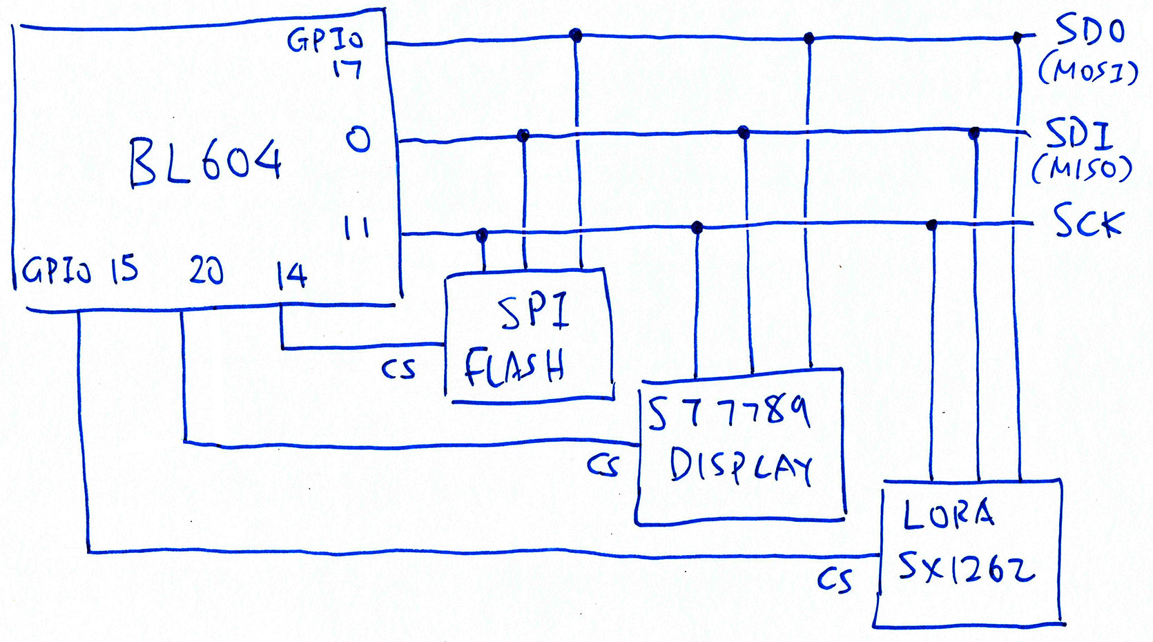
| GPIO Number | SPI Pin |
|---|---|
17 | Common SDO (MOSI) |
0 | Common SDI (MISO) |
11 | Common SCK |
14 | CS for SPI Flash |
20 | CS for ST7789 |
15 | CS for SX1262 |
UPDATE: There’s a new version of PineDio Stack BL604, the GPIO Numbers have changed
SPI Flash, ST7789 and SX1262 are connected to the same GPIO Pins for SDO (formerly MOSI), SDI (formerly MISO) and SCK.
But won’t BL604 get confused by the SPI crosstalk?
Nope because SPI Flash, ST7789 and SX1262 are connected to different Chip Select Pins.
When our firmware talks to an SPI Peripheral (like ST7789), we shall set the peripheral’s Chip Select Pin to Low.
(Our firmware shall set the Chip Select Pins to High when idle)
How shall we code the firmware for testing SPI?
The same way as BL602… By calling the BL602 / BL604 IoT SDK!
We start by defining the Shared GPIOs for the SPI Peripherals: pinedio_st7789/display.h
/// GPIO for ST7789 / SX1262 / SPI Flash SDO (MOSI)
#define DISPLAY_MOSI_PIN 17

/// GPIO for ST7789 / SX1262 / SPI Flash SDI (MISO)
#define DISPLAY_MISO_PIN  0

/// GPIO for ST7789 / SX1262 / SPI Flash SCK
#define DISPLAY_SCK_PIN  11
Followed by the Chip Select GPIOs for each SPI Peripheral…
/// GPIO for SPI Flash Chip Select. We must set this to High to deselect SPI Flash.
#define FLASH_CS_PIN 14
/// GPIO for SX1262 SPI Chip Select. We must set this to High to deselect SX1262.
#define SX1262_CS_PIN 15
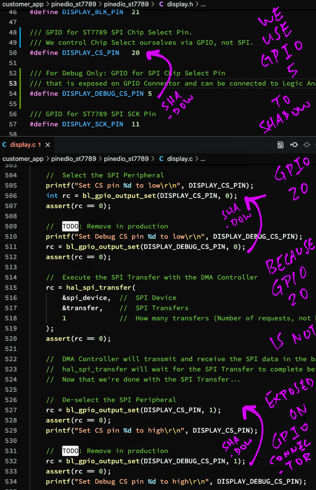
/// GPIO for ST7789 SPI Chip Select. We control Chip Select ourselves via GPIO, not SPI.
#define DISPLAY_CS_PIN 20The SPI Functions from the BL604 IoT SDK need us to specify a Chip Select GPIO.
Since we’re controlling Chip Select ourselves, we’ll assign GPIO 8 as the Unused Chip Select…
/// GPIO for unused SPI Chip Select Pin. Unused because we control Chip Select ourselves via GPIO, not SPI.
#define DISPLAY_UNUSED_CS_PIN 8

/// For Debug Only: GPIO for SPI Chip Select Pin that is exposed on GPIO Connector and can be connected to Logic Analyser
#define DISPLAY_DEBUG_CS_PIN 5

/// GPIO for Backlight
#define DISPLAY_BLK_PIN  21
(GPIO 8 selects the Flashing Mode when BL604 is booting, so GPIO 8 is normally unused)
We use GPIO 5 to mirror the GPIO High / Low State of GPIO 20 (ST7789 Chip Select). More about this in a while.
Let’s initialise the SPI Port before sending data: pinedio_st7789/demo.c
/// Command to init the display
static void test_display_init(char *buf, int len, int argc, char **argv) {
  //  Configure Chip Select, Backlight pins as GPIO Output Pins (instead of GPIO Input)
  int rc;
  rc = bl_gpio_enable_output(DISPLAY_BLK_PIN, 0, 0);  assert(rc == 0);
  rc = bl_gpio_enable_output(DISPLAY_CS_PIN,  0, 0);  assert(rc == 0);
  rc = bl_gpio_enable_output(FLASH_CS_PIN,    0, 0);  assert(rc == 0);
  rc = bl_gpio_enable_output(SX1262_CS_PIN,   0, 0);  assert(rc == 0);
  rc = bl_gpio_enable_output(DISPLAY_DEBUG_CS_PIN, 0, 0);  assert(rc == 0);
First we configure the Chip Select GPIOs for GPIO Output (instead of GPIO Input).
Next we set the Chip Select GPIOs to High to deselect all SPI Peripherals…
  //  Set Chip Select pins to High, to deactivate SPI Flash, SX1262 and ST7789
  rc = bl_gpio_output_set(FLASH_CS_PIN,   1);  assert(rc == 0);
  rc = bl_gpio_output_set(SX1262_CS_PIN,  1);  assert(rc == 0);
  rc = bl_gpio_output_set(DISPLAY_CS_PIN, 1);  assert(rc == 0);
  rc = bl_gpio_output_set(DISPLAY_DEBUG_CS_PIN, 1);  assert(rc == 0);

  //  Switch on the backlight
  rc = bl_gpio_output_set(DISPLAY_BLK_PIN, 0); assert(rc == 0);

  //  Note: We must swap SDO (MOSI) and
  //  SDI (MISO) to comply with the
  //  SPI Pin Definitions in BL602 / BL604
  //  Reference Manual
  rc = GLB_Swap_SPI_0_MOSI_With_MISO(ENABLE);  assert(rc == 0);
(We’ll cover GLB_Swap_SPI in a while)
Finally we configure the SPI Port…
  //  Configure the SPI Port
  rc = spi_init(
    &spi_device, //  SPI Device
    SPI_PORT,    //  SPI Port
    0,           //  SPI Mode: 0 for Controller (formerly Master), 1 for Peripheral (formerly Slave)
    0,           //  SPI Polar Phase. Valid values: 0 (CPOL=0, CPHA=0), 1 (CPOL=0, CPHA=1), 2 (CPOL=1, CPHA=0) or 3 (CPOL=1, CPHA=1)
    1 * 1000 * 1000,  //  SPI Frequency (1 MHz, reduce this in case of problems)
    2,   //  Transmit DMA Channel
    3,   //  Receive DMA Channel
    DISPLAY_SCK_PIN,        //  SPI Clock Pin
    DISPLAY_UNUSED_CS_PIN,  //  Unused SPI Chip Select Pin (Unused because we control the GPIO ourselves as Chip Select Pin)
    DISPLAY_MOSI_PIN,       //  SPI Serial Data Out Pin (formerly MOSI)
    DISPLAY_MISO_PIN        //  SPI Serial Data In Pin  (formerly MISO) (Unused for ST7789)
  );
  assert(rc == 0);

  //  Note: DISPLAY_UNUSED_CS_PIN must NOT be the same as DISPLAY_CS_PIN.
  //  Because the SPI Pin Function will override the GPIO Pin Function!
We’re ready to transfer data over SPI!
Here’s how we transfer data (transmit + receive) over SPI: pinedio_st7789/display.c
/// Write packed data to the SPI port. `data` is the array of bytes to be written. `len` is the number of bytes.
static int transmit_packed(const uint8_t *data, uint16_t len) {
  //  Clear the receive buffer
  memset(&spi_rx_buf, 0, sizeof(spi_rx_buf));

  //  Prepare SPI Transfer
  static spi_ioc_transfer_t transfer;
  memset(&transfer, 0, sizeof(transfer));
  transfer.tx_buf = (uint32_t) data;        //  Transmit Buffer
  transfer.rx_buf = (uint32_t) spi_rx_buf;  //  Receive Buffer
  transfer.len    = len;                    //  How many bytes
Here we specify the Transmit Buffer and Receive Buffer for the SPI transfer.
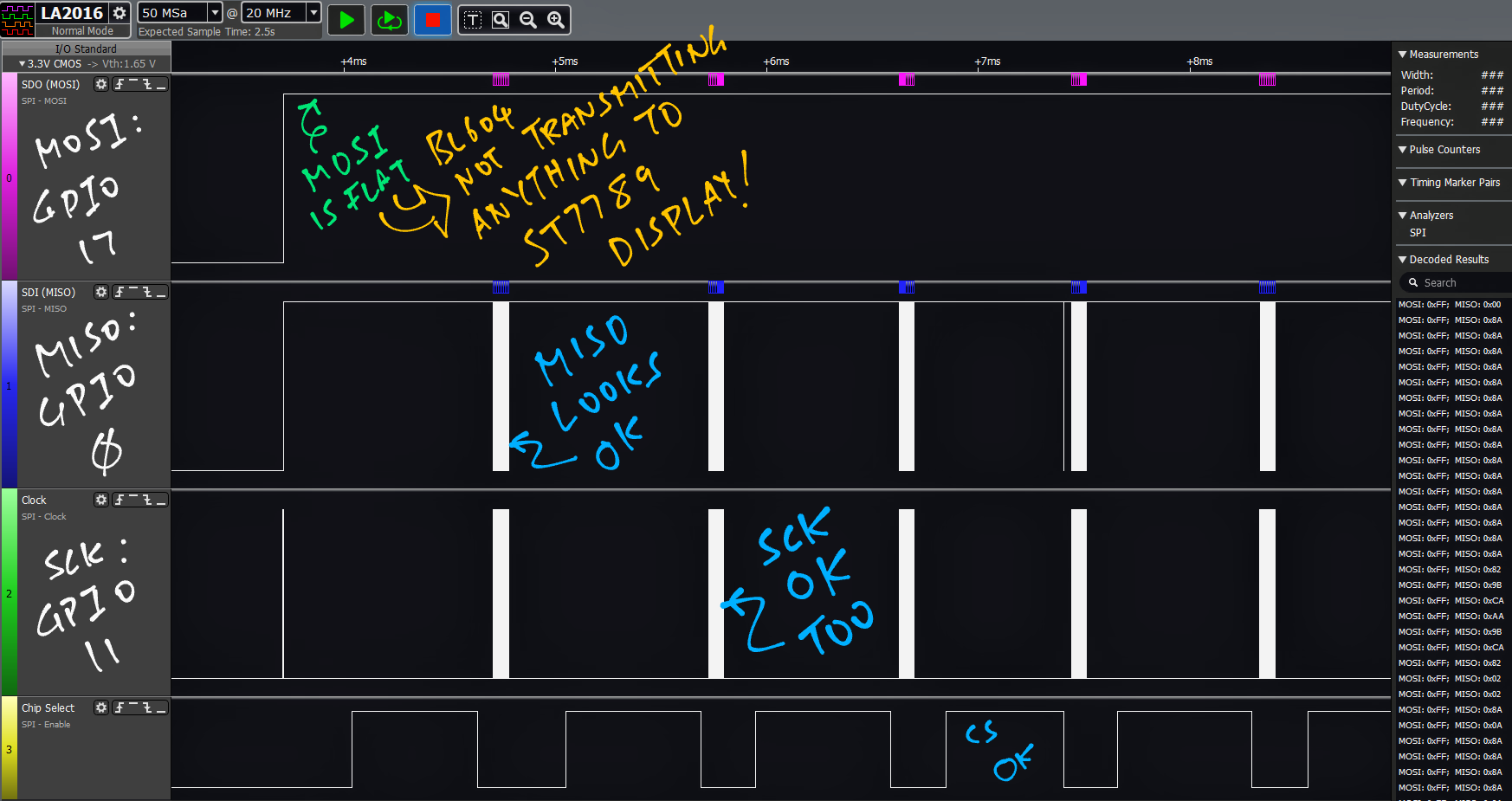
Next we set Chip Select GPIO to Low to select the SPI Peripheral (ST7789 Display)…
  //  Select the SPI Peripheral
  int rc;
  rc = bl_gpio_output_set(DISPLAY_CS_PIN, 0);        assert(rc == 0);
  rc = bl_gpio_output_set(DISPLAY_DEBUG_CS_PIN, 0);  assert(rc == 0);
Then we start the SPI Transfer (transmit + receive) and wait for it to complete…
  //  Execute the SPI Transfer with the DMA Controller
  rc = hal_spi_transfer(
    &spi_device,  //  SPI Device
    &transfer,    //  SPI Transfers
    1             //  How many transfers (Number of requests, not bytes)
  );
  assert(rc == 0);

  //  DMA Controller will transmit and receive the SPI data in the background.
  //  hal_spi_transfer will wait for the SPI Transfer to complete before returning.
Finally we set Chip Select GPIO to Low to deselect the SPI Peripheral (ST7789 Display)…
  //  Now that we're done with the SPI Transfer...
  //  Deselect the SPI Peripheral
  rc = bl_gpio_output_set(DISPLAY_CS_PIN, 1);        assert(rc == 0);
  rc = bl_gpio_output_set(DISPLAY_DEBUG_CS_PIN, 1);  assert(rc == 0);
  return 0;
}
That’s how we transmit and receive data over SPI!
Why did we use BL604’s Direct Memory Access (DMA) Controller for the SPI Transfer?
Because we want the SPI Transfer to be executed in the background, freeing up the CPU for other concurrent tasks.
BL604’s DMA Controller executes the SPI Transfer on behalf of the CPU, shuffling data between the Transmit / Receive Buffers and the SPI Peripheral (ST7789).
What is DISPLAY_DEBUG_CS_PIN? Why is it mirroring DISPLAY_CS_PIN?
Yep everything we do to DISPLAY_CS_PIN (GPIO 20), we do the same to DISPLAY_DEBUG_CS_PIN (GPIO 5).
We’ll learn why in the next chapter.
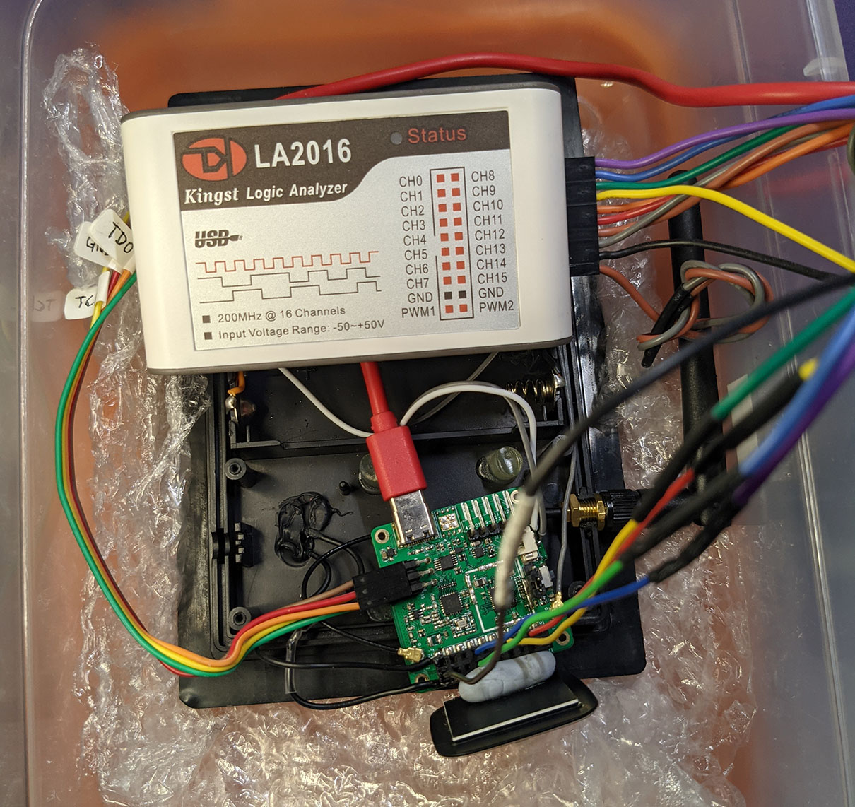
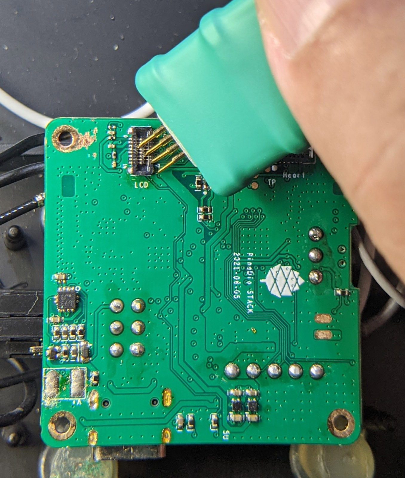
When testing Prototype Hardware… Always have a Logic Analyser ready! (Pic above)
Why? Because we’ll hit a baffling signalling problem when we test SPI on PineDio Stack.
How do we capture the data transferred over the SPI Port?
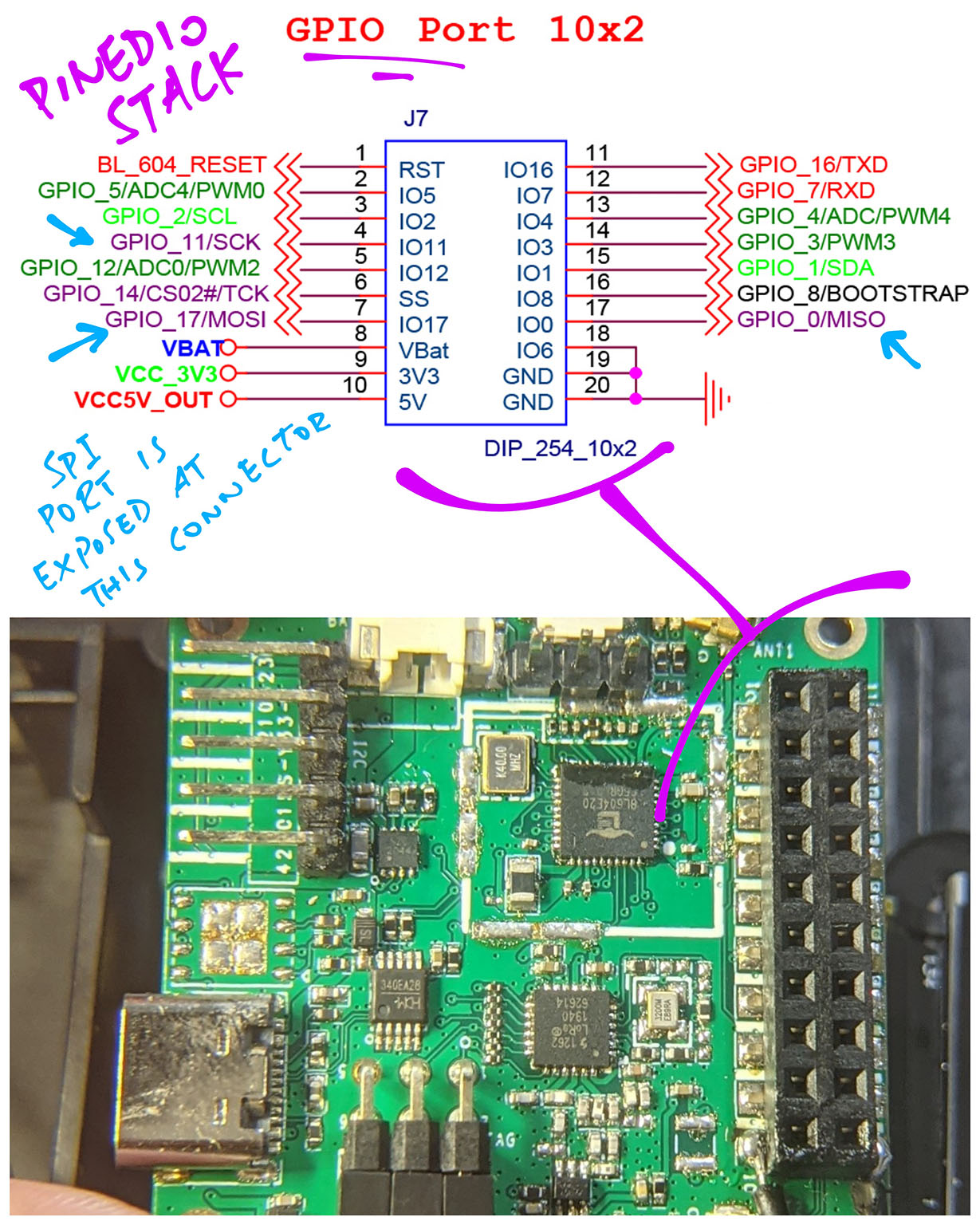
PineDio Stack’s GPIO Connector (at right) exposes the SPI Pins: SDO (formerly MOSI), SDI (formerly MISO) and SCK
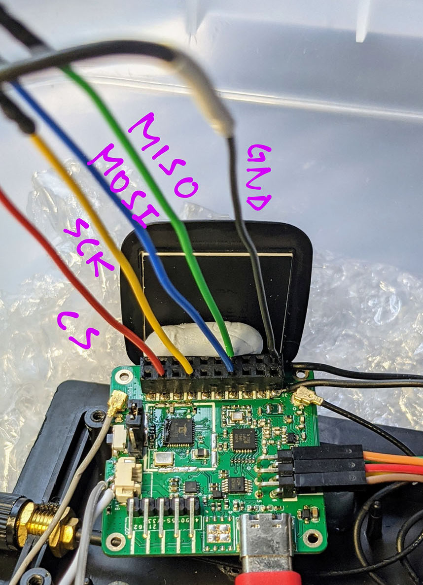
We connect our Logic Analyser to the GPIO Connector like so…
| GPIO Number | SPI Pin | Connector Pin |
|---|---|---|
17 | Common SDO (MOSI) | 7 |
0 | Common SDI (MISO) | 17 |
11 | Common SCK | 4 |
5 | Debug CS | 2 |
UPDATE: There’s a new version of PineDio Stack BL604, the GPIO Numbers have changed
What about the ST7789 Chip Select Pin: GPIO 20?
Unfortunately GPIO 20 is not exposed on the GPIO Connector.
But remember: Everything we do to GPIO 20, we do the same to GPIO 5!
GPIO 5 is exposed on the GPIO Connector and it mirrors the GPIO High / Low state of GPIO 20.
Thus we simply connect our Logic Analyser to GPIO 5 as the Chip Select Pin! (Pic above)
Let’s look at the data collected by our Logic Analyser…
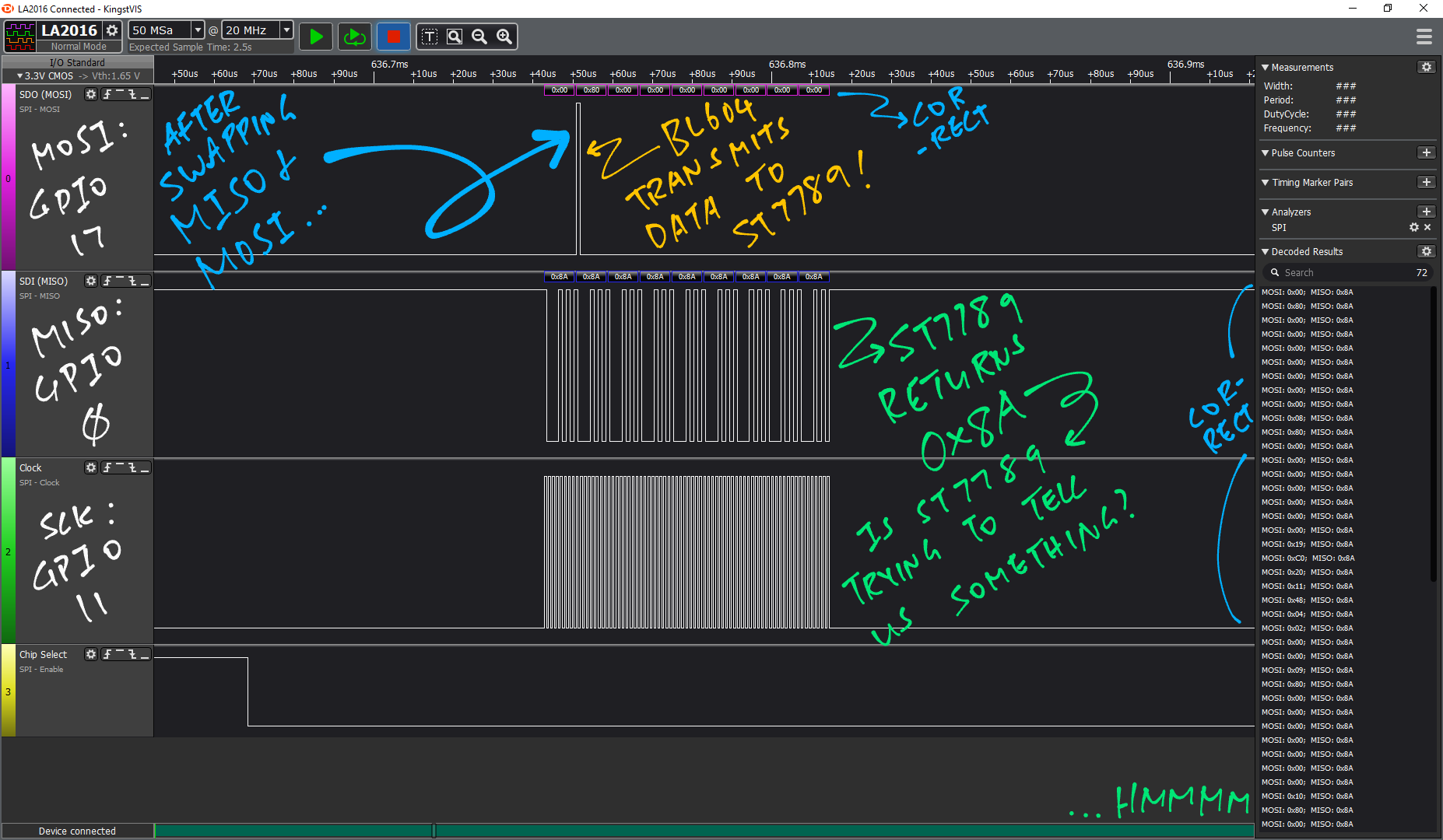
What appears in the Logic Analyser when BL604 transmits data over SPI?
Watch what happened the very first time that we transmitted SPI data from BL604 to ST7789 Display…
The top line showed that SDO (MOSI) was flat…
No data was flowing out from BL604 to ST7789 Display!
Though SDI (MISO) looked OK…
Maybe SDO and SDI were swapped?
Thankfully JF found the fix!
//  Note: We must swap SDO (MOSI) and
//  SDI (MISO) to comply with the
//  SPI Pin Definitions in BL602 / BL604
//  Reference Manual
int rc = GLB_Swap_SPI_0_MOSI_With_MISO(ENABLE); assert(rc == 0);After applying the fix, BL604 swaps the SDO and SDI pins… And BL604 transmits SPI data correctly to ST7789!
But the BL604 Reference Manual says that GPIO 17 is SDO (MOSI)… Not SDI (MISO) right?
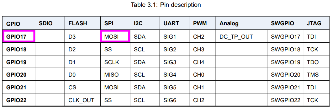
Yeah the BL604 Reference Manual says that GPIO 17 is SDO (MOSI)… So we shouldn’t need to call GLB_Swap_SPI_0_MOSI_With_MISO to swap the pins.
But since PineDio Stack was designed for GPIO 17 as SDO (MOSI), we’ll have to call GLB_Swap_SPI_0_MOSI_With_MISO in our firmware to make SPI work.
This SPI Pin Swap Problem sounds familiar…?
Yep if you’ve been following my BL602 Adventures, we’ve seen this SPI Pin Swap Problem on BL602…
Hence I’m happy to confirm: BL604 is 100% compatible with BL602… Right down to the SPI Quirks!
How does this SPI Pin Swap Problem affect PineDio Stack Developers?
To work around the SPI Pin Swap Problem…
All PineDio Stack Developers should ensure that GLB_Swap_SPI_0_MOSI_With_MISO is always called before initialising the SPI Port.
Now that PineDio Stack SPI is OK, let’s draw something on the ST7789 Display!
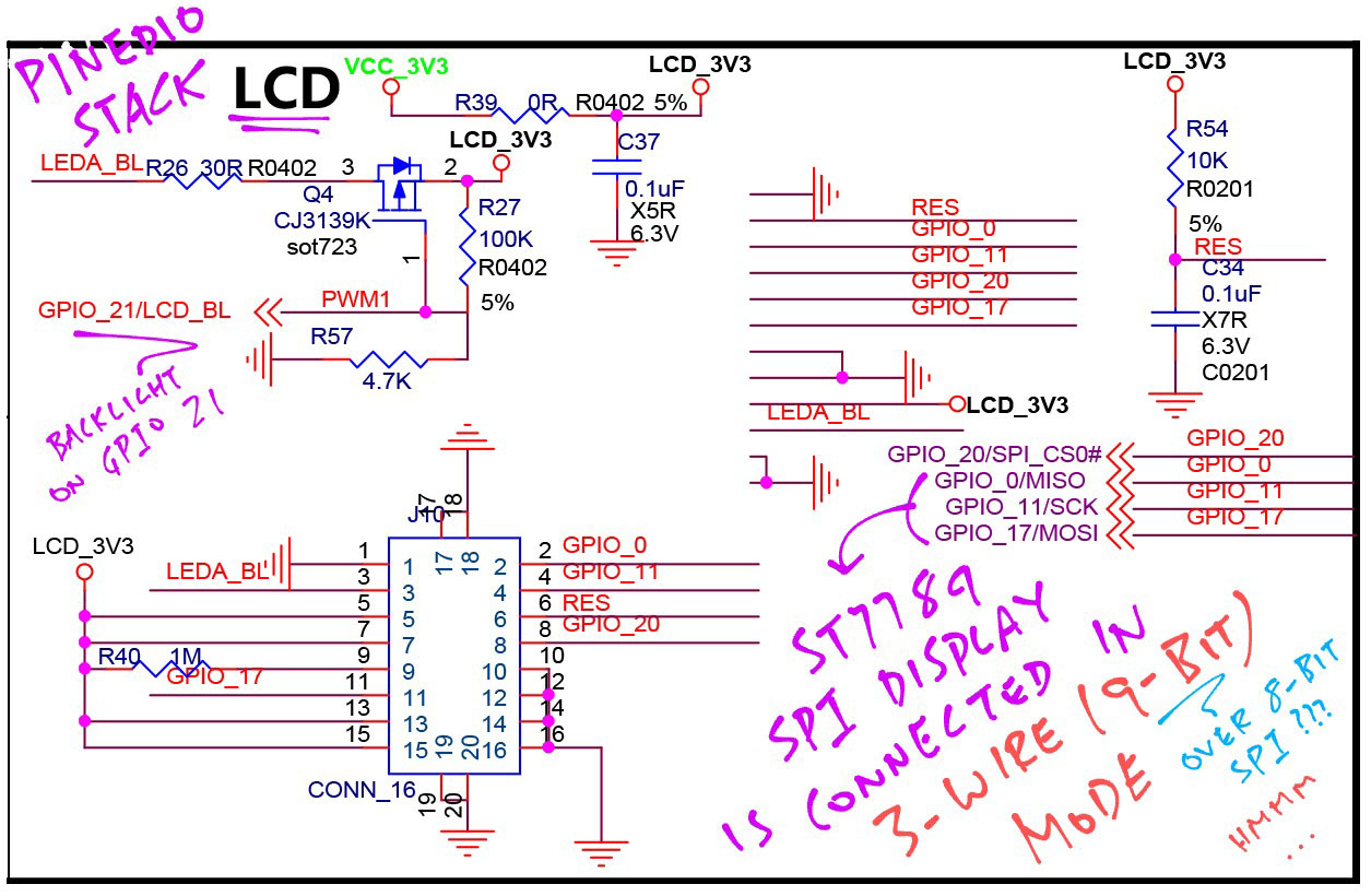
According to the PineDio Stack Schematic…
The ST7789 SPI Display is connected on these pins…
GPIO 20: SPI Chip Select
GPIO 0: SPI SDI (MISO)
GPIO 11: SPI SCK
GPIO 17: SPI SDO (MOSI)
UPDATE: There’s a new version of PineDio Stack BL604, the GPIO Numbers have changed
Wait are we missing a pin?
Yep we usually connect the ST7789 Data / Command (DC) Pin. (Like on PineTime)
We flip this pin to Low to indicate that we’re sending Command Bytes, and flip it to High for Data Bytes.
We call this the 4-Wire Interface for ST7789: SDO, SDI, SCK and DC.
Data / Command (DC) Pin is missing on PineDio Stack. So we’re using the 3-Wire Interface?
Yep ST7789 supports a 3-Wire Interface: SDO, SDI and SCK. (Without DC)
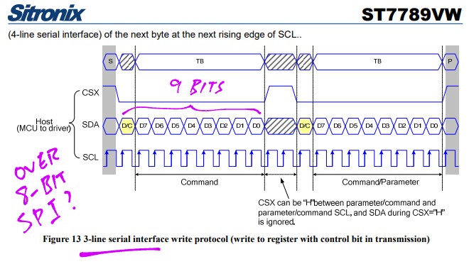
Instead of transmitting the Data / Command Indicator on a separate pin, the 3-Wire Interface inserts a Data / Command (DC) Bit to specify whether the upcoming byte is a Command or Data Byte.
(DC Bit is 1 for Command Byte, 0 for Data Byte)
Whoa that means we transmit 9 bits for every Data and Command Byte?
Yep we need to find some way to transmit 9-bit data over our 8-bit SPI Port.
The 3-Wire (9-bit) Interface might actually be more efficient than the 4-Wire (8-bit) Interface… Because it lets us blast out multiple Command and Data Bytes in a single SPI DMA Transfer.
(Without having to flip the Data / Command Pin)
More about this in the next chapter.
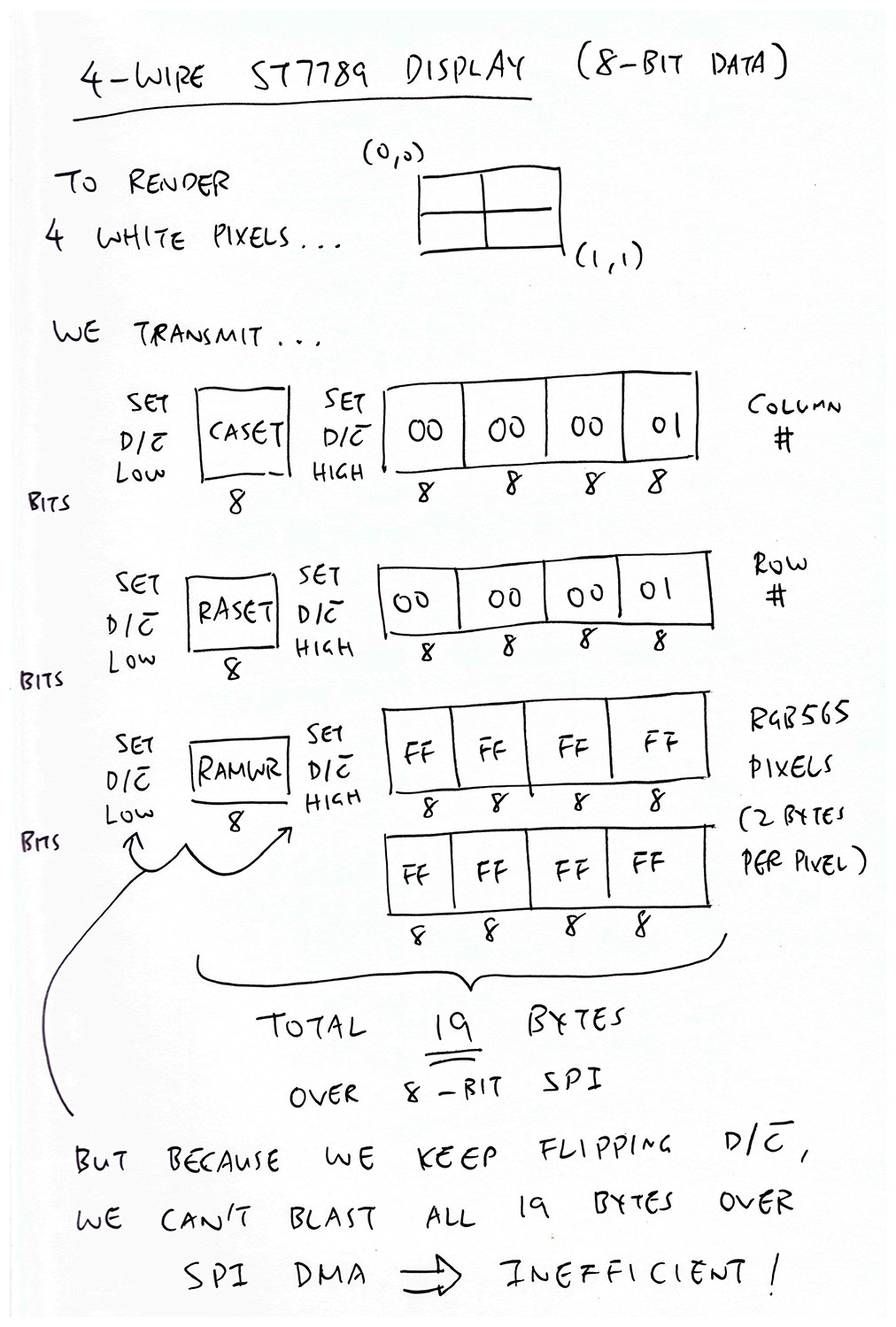
Why can’t we stick with the familiar 4-Wire Interface for ST7789?
I guess the PineDio Stack hardware designers wanted to free up a precious GPIO Pin for use by other components.
(And maybe the designers also thought that the 3-Wire Interface is more efficient than the 4-Wire one!)
How on earth do we send 9-bit data over 8-bit SPI to ST7789 Display?
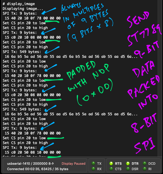
OK hear me out… We could pack the 9-bit data into chunks of 9 bytes. Then send the chunks over 8-bit SPI.
(Why 9 bytes? Because 9 bytes = 9 bits x 8)
What if the 9-bit data doesn’t fill up a 9-byte chunk?
We fill up the rest of the chunk with the ST7789 NOP Command Byte (0x00).
Show me how?
Previously we did this for the 4-Wire (8-bit) ST7789 Interface…
Now we do this for the 3-Wire (9-bit) ST7789 Interface…
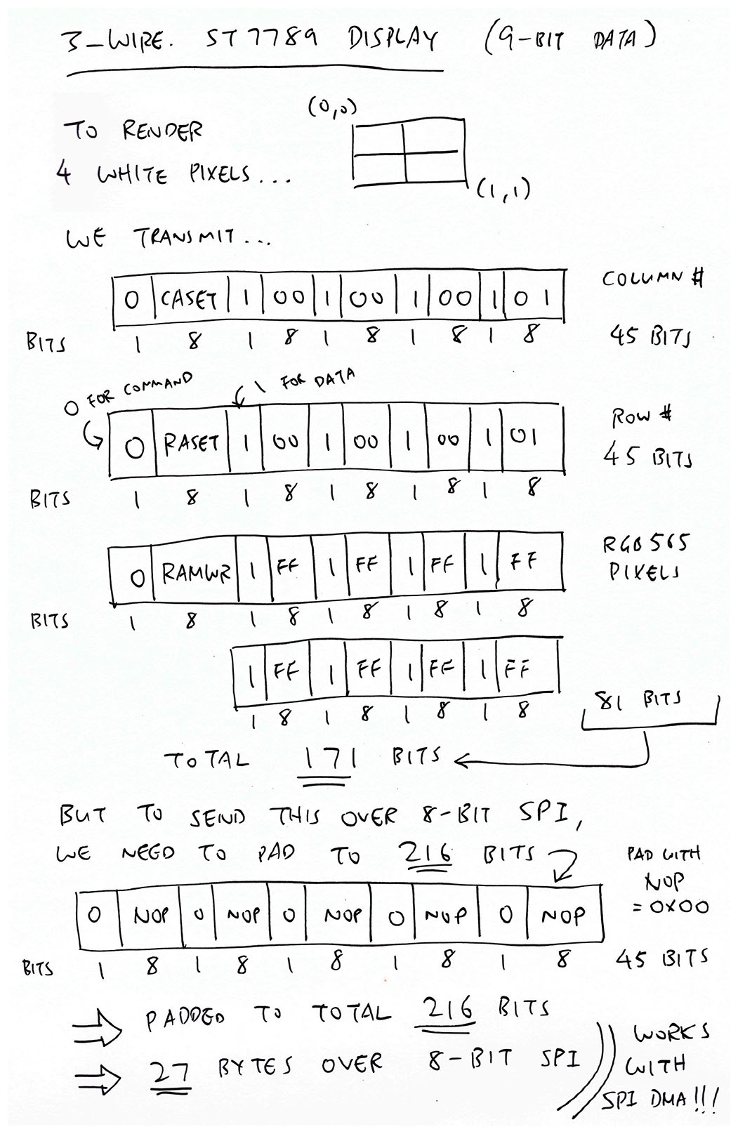
Thus we’re sending 8-bit data over SPI… But it magically appears as 9-bit data to ST7789!
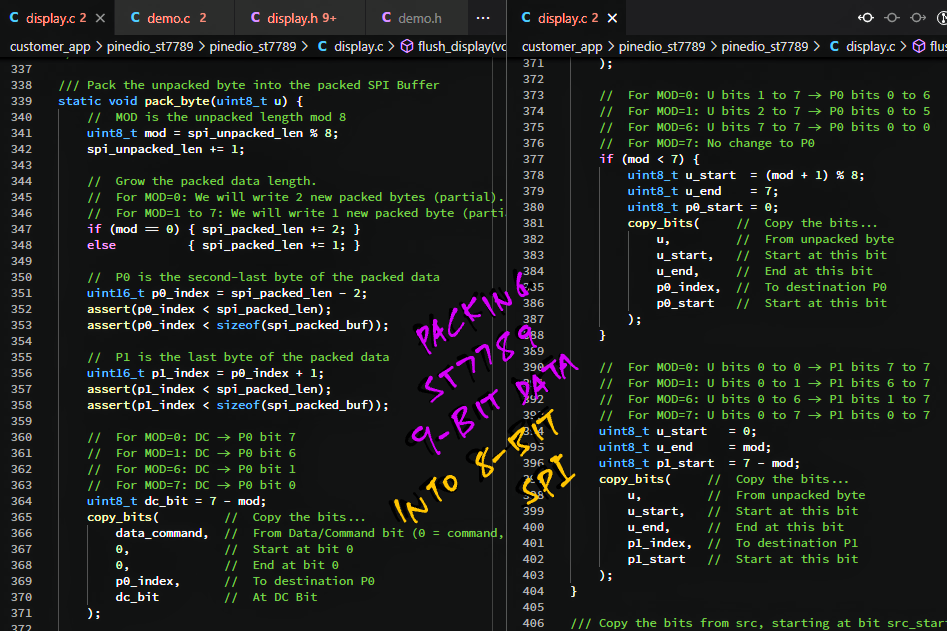
How exactly do we pack 9-bit data into chunks of 9 bytes?
Here’s the 9-Bit Packing Logic (please pardon my peculiar pseudocode)…
To pack 9-bit data into bytes, we do this for every 8 bytes of unpacked data (Most Significant Bit first)…
If Unpacked Length mod 8 is…
0:
DC → P0 bit 7
U bits 1 to 7 → P0 bits 0 to 6
U bits 0 to 0 → P1 bits 7 to 7
1:
DC → P0 bit 6
U bits 2 to 7 → P0 bits 0 to 5
U bits 0 to 1 → P1 bits 6 to 7
2:
DC → P0 bit 5
U bits 3 to 7 → P0 bits 0 to 4
U bits 0 to 2 → P1 bits 5 to 7
…
6:
DC → P0 bit 1
U bits 7 to 7 → P0 bits 0 to 0
U bits 0 to 6 → P1 bits 1 to 7
7:
DC → P0 bit 0
U bits 0 to 7 → P1 bits 0 to 7
Where…
The implementation looks like this…
Since the 9-Bit Packing is implemented in C, let’s test it on Linux!
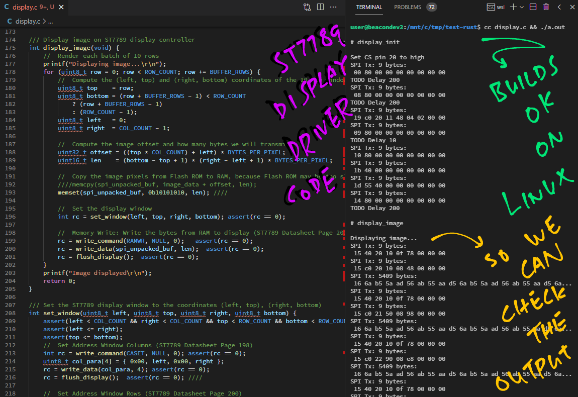
We verify the packed data with this spreadsheet…
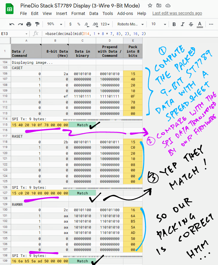
Sadly nope.
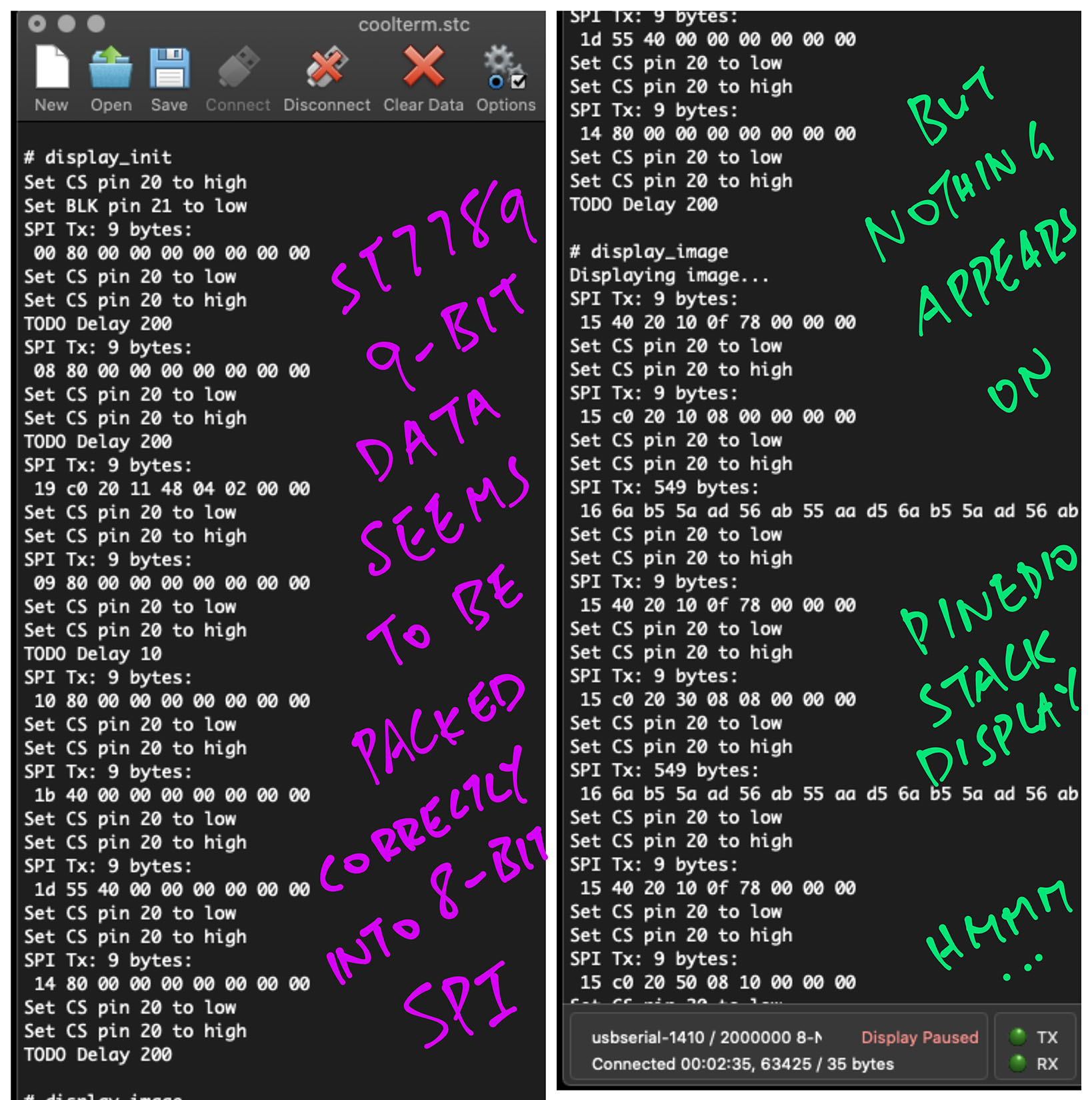
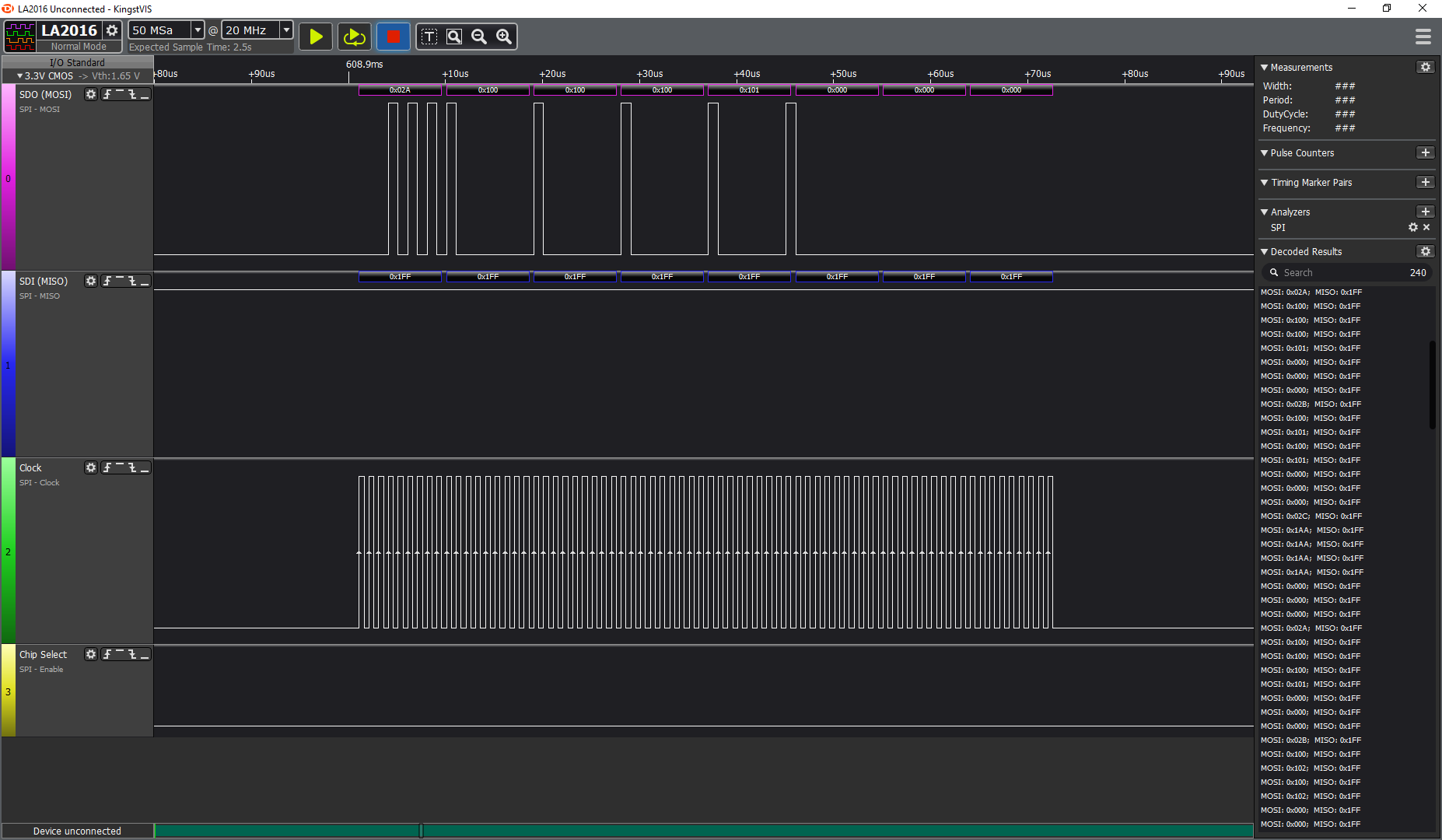
Our 9-bit data is correctly packed into 9-byte chunks and sent to ST7789 over SPI…
Yet nothing appears on the ST7789 Display.
We also verified the SPI Data with our Logic Analyser and its 9-bit SPI Decoder…
Are we being too smarty-pants with 9-bit SPI? Like adding feet to a drawing of a snake?
Let’s talk to ST7789 the simpler way… With Bit-Banging! (Instead of SPI)
moononournation has built an awesome Arduino GFX Library that supports 9-Bit-Banging to ST7789 Display…
Let’s port this Arduino Library to BL604!
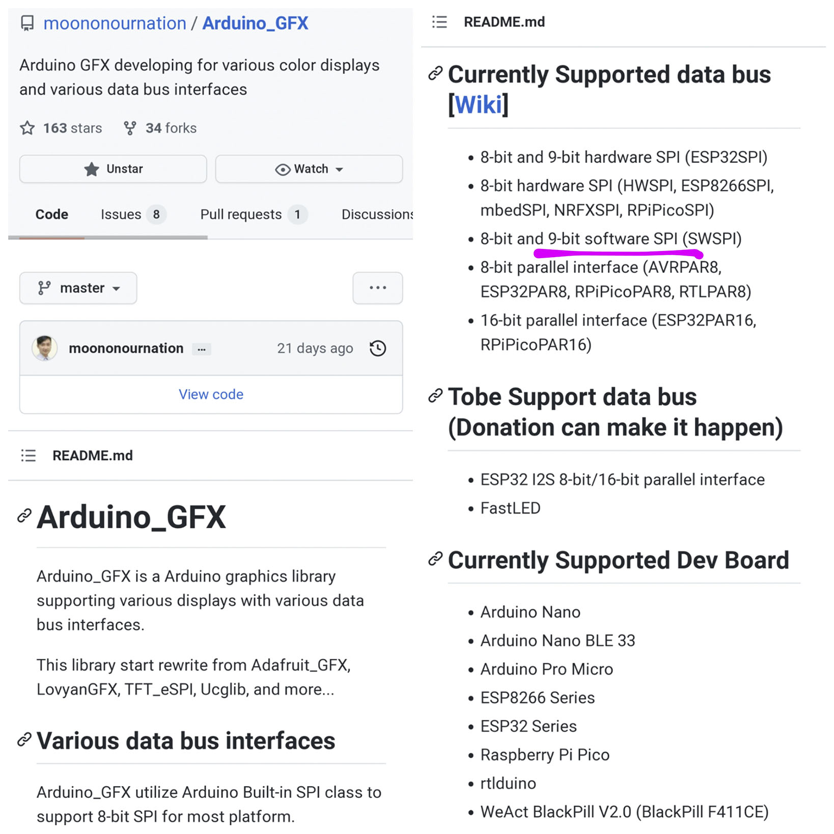
We ported only two source files from Arduino GFX Library to BL604…
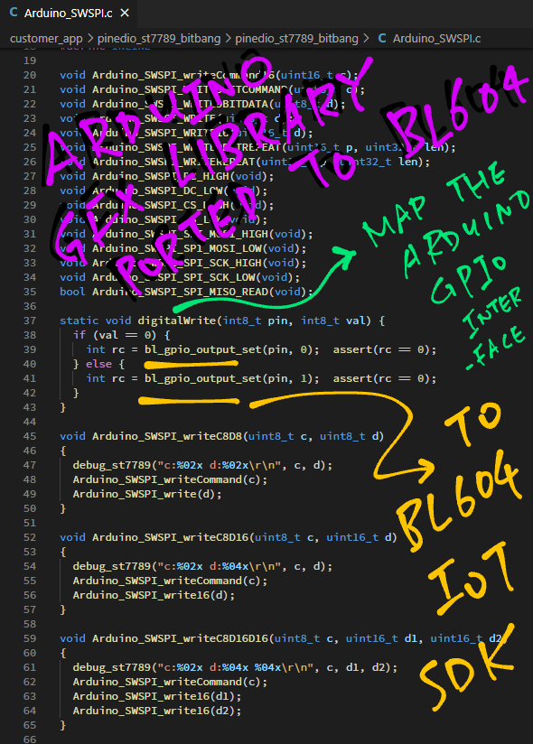
…By mapping the Arduino API to BL604 IoT SDK.
(And we flattened the C++ Classes into plain C Functions)
Our Logic Analyser shows that the 9-bit ST7789 data is correctly Bit-Banged to ST7789…
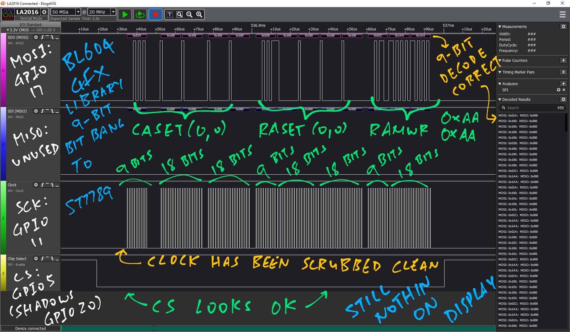
(We’re using the 9-Bit SPI Decoder with our Logic Analyser)
Guess what? Nothing appears on PineDio Stack’s ST7789 Display! 😭
To be super sure, we tested Arduino GFX on Linux and verified the data…
Now we’re super stuck with our ST7789 testing!
Wait a minute… Is there a switch that configures ST7789 Display for 3-Wire or 4-Wire Interface?
Pins IM0 to IM3 on ST7789 will select the 3-Wire or 4-Wire Interface…
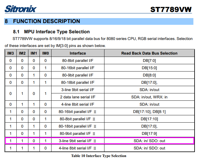
So for 3-Wire (9-Bit) Interface, we should hardwire the pins as…
| IM3 | IM2 | IM1 | IM0 |
|---|---|---|---|
1 | 1 | 0 | 1 |
Maybe Pins IM0 to IM3 are not hard-wired as such?
That’s a possibility… Which we’re checking with the Display Makers now.
Also we’re probing the tiny ST7789 Connector (with a sharp Pogo Pin) to understand how the pins are connected.
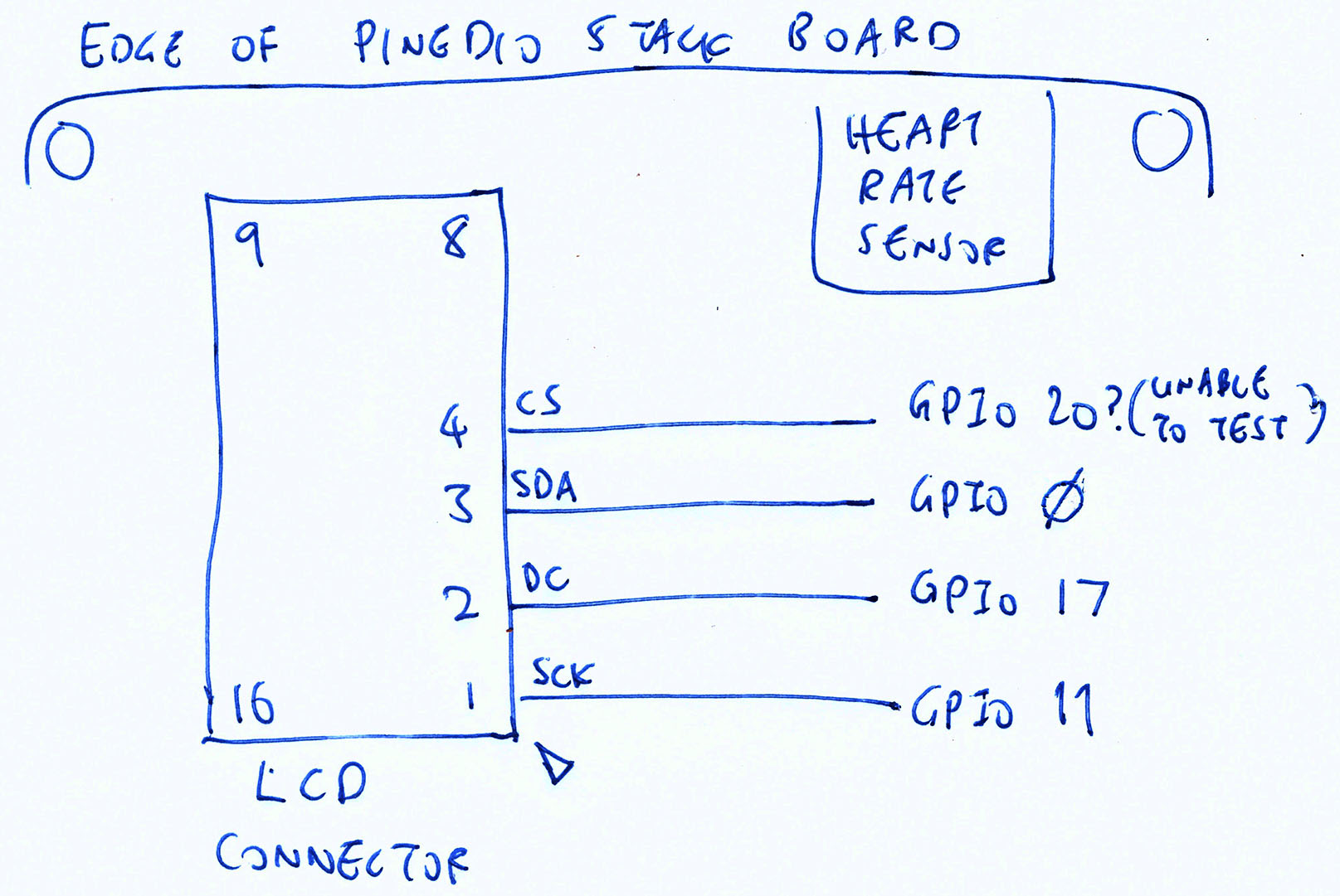
Here’s what we discovered from the Pogo Pin Probing…
| ST7789 Pin | BL604 GPIO |
|---|---|
| SDA | GPIO 0 |
| DC | GPIO 17 |
| SCK | GPIO 11 |
UPDATE: There’s a new version of PineDio Stack BL604, the GPIO Numbers have changed
Not quite what we expected. We tried both SPI and Bit-Banging with the discovered settings…
But both don’t show anything on the ST7789 Display.
We also tried to read the display ID (RDDID) by flipping GPIO 0 between output and input modes…
But the GPIO 0 signal looks glitchy. See the top line, centre part…
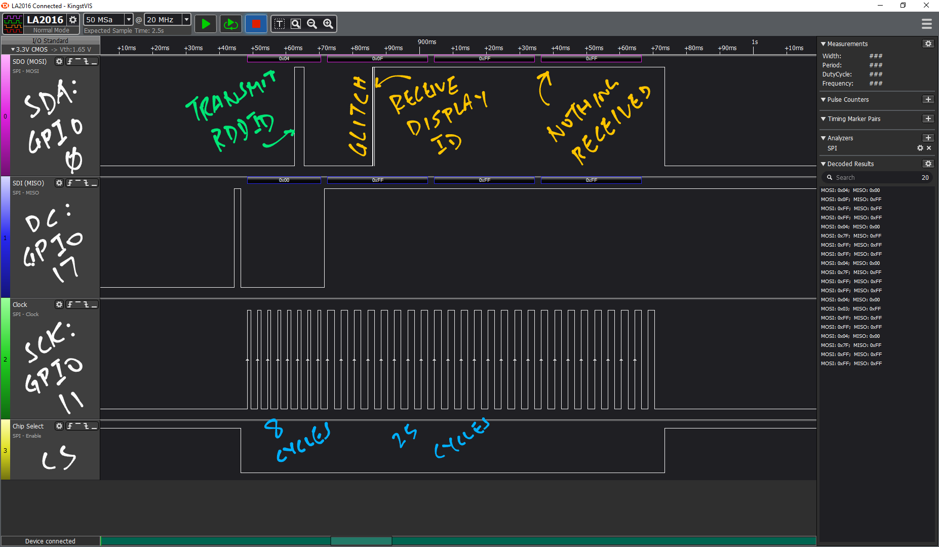
Any ideas? 🤔
UPDATE: JF commented…
About the serial modes of the ST7789, my understanding is that it supports 4 modes :
- 2 “interface” (I and II) : “I “ means that the same pin (SDA in the datasheet) is used as data INPUT and OUTPUT. “II” means it uses 1 pin as INPUT (SDA) and one as OUTPUT (SDO)
- 3/4 lines : 3 lines means that the driver must output 9 bits for each “byte” sent to the driver (the 9th bit being the data/command bit). In 4 lines, the 4th lines is used to output the data/command bit, allowing the driver to send 8-bits “bytes” on the SPI bus.
The mode implemented on the PineTime and on this LCD board is the “4-lines interface I” : data/command pin + single MOSI -> SDA pin as data pin. I think we could use the 4-lines interface II mode if we wanted to read data from the display (MOSI -> SDA, MISO -> SDO), but that is not necessary.
The naming of the pins in the datasheet are really confusing : the controller is advertised (and works) as a SPI device, but the pins are labelled as I²C pins. However, I do confirm that I’m driving the controller using the SPI bus, not the I²C!
See JF’s experiment with PineDio Stack and an external ST7789 display
I’m really excited that PineDio Stack BL604 will be available soon!
But in the meantime, JF and I have plenty to test on PineDio Stack…
Please let us know if you’re keen to help! 🙏
UPDATE: LoRa SX1262 on PineDio Stack has been tested OK! See this article…
Many Thanks to @moononournation and @AndreasDyhrberg for the valuable tips on testing PineDio Stack BL604!
This has been a super exciting first week of testing the Prototype Hardware for PineDio Stack BL604…
I hope you will join JF and me as we continue our testing of PineDio Stack.
(Maybe real soon we’ll create toasters, microwave ovens and pressure cookers with PineDio Stack!)
Got a question, comment or suggestion? Create an Issue or submit a Pull Request here…
lupyuen.github.io/src/pinedio.md
This article is the expanded version of this Twitter Thread
JF has successfully tested PineDio Stack’s SPI Port with an external eInk Display
We have created new firmware to Bit-Bang ST7789’s 4-Wire (8-Bit) Interface: pinedio_st7789_bitbang2
Sometimes we need to restart PineDio Stack to see the Boot Messages, without disconnecting the USB port. Here’s how…
We assume that PineDio Stack is already powered on by our computer (via USB)
Connect a Jumper Cable between Pin 5 (GND) and Pin 6 (RESET) of the JTAG Port (Pic above)
Disconnect the Jumper Cable
PineDio Stack will restart. The Boot Messages will appear in the Serial Terminal.