📝 2 Oct 2022
UPDATE: Apache NuttX RTOS now supports MIPI DSI! (See this)
How does Pine64 PinePhone control its LCD Display?
Let’s uncover all the secrets about PinePhone’s mysterious LCD Display and its MIPI Display Serial Interface…
What’s a MIPI Display Serial Interface (DSI)
What’s inside PinePhone’s LCD Display
How it’s similar to PineTime’s ST7789 Display Controller
One lane for Commands, but 4 lanes for Data!
Implications of a RAM-less Display Controller
What are PinePhone’s Display Engine (DE) and Timing Controller (TCON)
Why are we doing this?
We’re now porting Apache NuttX RTOS to PinePhone.
But it will look awfully dull until we render something on PinePhone’s LCD Display!
That’s why we’re probing the internals of PinePhone to create a NuttX Display Driver.
We’ll come back to this. Let’s continue the journey from our NuttX Porting Journal…
PineTime Smartwatch with ST7789 Display Controller
Why PineTime Smartwatch? Is it really similar to PinePhone’s Display?
Sounds unbelievable, but PineTime’s ST7789 Display Controller has plenty in common with PinePhone’s Display!
(Think of PinePhone as a Super-Sized PineTime)
In this article we shall explain PinePhone’s Display by comparing it with PineTime.
A quick recap of PineTime’s ST7789 Display…
PineTime talks to its display over SPI (single data lane)…
(We’ll soon see that PinePhone talks to its display over 4 data lanes)
PineTime uses an extra pin to indicate whether it’s sending Commands or Pixel Data
(PinePhone won’t need this, we’ll learn why)
At startup, PineTime sends an Initialisation Sequence of Commands to initialise the display…
(PinePhone will send a similar Initialisation Sequence, but much longer)
PineTime renders a rectangular chunk of the display at a time…
(PinePhone will refresh its entire display continuously)
If we’re not familiar with PineTime’s ST7789 Display, please read the docs above!
We’ve read the docs, can we move on?
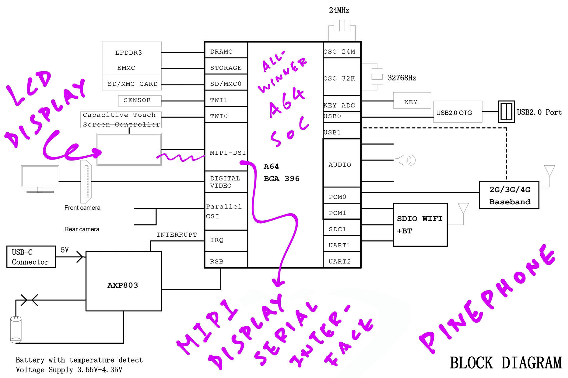
OK great! To understand how PinePhone’s Display differs from PineTime, we begin with the schematic…
LCD Display on PinePhone Schematic (Page 2)
Let’s turn to Page 2 of the PinePhone Schematic to understand how PinePhone’s Display is connected…
From the pic above, we see that the LCD Display is connected to the Allwinner A64 SoC via a MIPI Display Serial Interface (DSI).
(MIPI is the Mobile Industry Processor Interface Alliance)
What’s a MIPI Display Serial Interface?
Think of it as SPI, but supercharged with Multiple Data Lanes!
The (dull) technical details of DSI are covered here…
But if we’re seeking a gentler intro to DSI, please follow me to the next section…
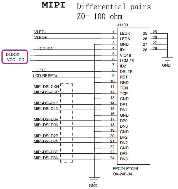
MIPI DSI Connector on PinePhone Schematic (Page 11)
How shall we learn about MIPI DSI?
We’ll learn plenty about MIPI DSI (Display Serial Interface)… Just by looking at PinePhone’s Connector for the LCD Display!
Flip to Page 11 of the PinePhone Schematic and we’ll see the MIPI DSI Connector. (Pic above)
The MIPI DSI Connector connects PinePhone’s Allwinner A64 SoC directly to the LCD Display. In the pic above we see these connections…
CKN and CKP are the DSI Clock Lines
(Similar to SPI Clock)
D0N and D0P for DSI Data Lane 0
(Similar to SPI MISO / MOSI)
D1N and D1P for DSI Data Lane 1
(Yep DSI has more data lanes than SPI)
D2N and D2P for DSI Data Lane 2
D3N and D3P for DSI Data Lane 3
(MIPI DSI has 4 data lanes!)
Why the N and P?
Because P=NP… Kidding!
N means Negative, P means Positive.
This means that MIPI DSI uses Differential Signalling for high-speed data transfers. (4.5 Gbps per lane)
(Differential Signalling is also used in HDMI and USB)
Are all 4 DSI Data Lanes identical?
For sending commands to the Display Controller, only DSI Lane 0 is used.
(Lane 0 is Bidirectional, it supports Direction Turnaround)
For sending pixel data, all 4 DSI Lanes will be used. (Unidirectional)
Let’s dig deeper into MIPI DSI…
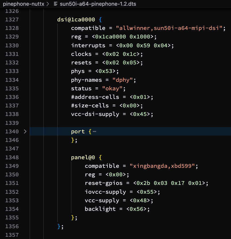
Xingbangda XBD599 in PinePhone’s Linux Device Tree
What’s connected to this MIPI DSI Connector?
The Linux Device Tree describes everything about PinePhone Hardware in a single text file. Let’s snoop around the Device Tree!
First we follow these steps to dump PinePhone’s Linux Device Tree in text format…
Then we search for MIPI DSI in the Device Tree…
From the pic above we see that PinePhone’s MIPI DSI Connector is connected to Xingbangda XBD599.
This is a 5.99-inch 720x1440 MIPI DSI IPS LCD Panel.
But what’s super interesting is that Xingbangda XBD599 has a Sitronix ST7703 LCD Controller inside!
Let’s probe deeper…
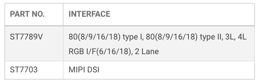
PineTime (ST7789) vs PinePhone (ST7703)
Sitronix ST7703 sounds familiar?
Yep Sitronix makes the LCD Controllers for BOTH PineTime and PinePhone!
In fact they’re from the same family of LCD Controllers. (ST7789 vs ST7703)
Just that PineTime uses an SPI Interface while PinePhone uses a MIPI DSI Interface. (Pic above)
The resolutions are different too. PinePhone has a huge display with more colours…
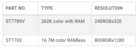
Which means that PinePhone’s LCD Controller is RAM-less…
It doesn’t have any RAM inside to remember the pixels. (Unlike PineTime)
What’s the implication of a RAM-less display?
Because PinePhone’s LCD Controller doesn’t have any RAM inside to remember the pixels drawn…
PinePhone’s A64 SoC will pump a constant stream of pixels to refresh the display.
(Just like an old CRT TV!)
This pixel pumping is done by A64’s Display Engine (DE) and Timing Controller (TCON0). We’ll come back to this.
What happens inside PinePhone’s ST7703 LCD Controller?
Let’s figure out by looking at the initialisation of PinePhone’s ST7703 LCD Controller.
Xingbangda has provided an Initialisation Sequence of (magical) ST7703 Commands that we should send to the LCD Controller at startup…
| Byte | Purpose |
|---|---|
B9 | SETEXTC: Enable USER Command (Page 131) |
F1 | - Enable USER Command |
12 | - (Continued) |
83 | - (Continued) |
BA | SETMIPI: Set MIPI Registers (Page 144) |
33 | - Virtual Channel (0), Number of Lanes (4) |
81 | - LDO Voltage, Terminal Resistance |
05 | - MIPI Low High Speed driving ability |
F9 | - TXCLK speed in DSI LP mode |
0E | - Minimum HFP number |
0E | - Minimum HBP number |
| … | (And many more commands, see this list) |
The above commands are (mostly) documented in the ST7703 Datasheet…
How to send the Init Sequence to ST7703?
We’ll send the above commands to ST7703 via a MIPI DSI Display Command: DCS Long Write.
Which we’ll explain next…
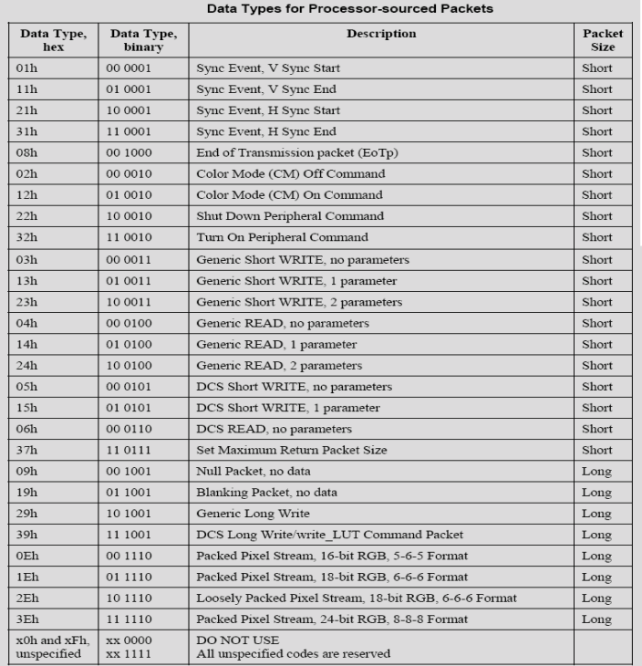
MIPI DSI Display Command Set from A31 User Manual (Page 837)
MIPI Display Serial Interface (DSI) defines a standard list of commands for controlling the display: DSI Display Command Set (DCS). (Pic above)
To send the Initialisation Sequence to ST7703, we shall transmit the DCS Long Write command. (Data Type 0x39)
Which is described in the ST7703 Datasheet (page 19)…
Display Command Set (DCS) Long Write is always using a Long Packet from the HOST to the driver IC.
The content can include Command (No Parameters) or Command with 1 or more parameters.
(More about “Long Packet” in a while)
And we shall transmit the DCS Long Write command in DSI Video Mode.
Let’s talk about DSI Video Mode…
(Note: We might need to use DCS Short Write No Parameters 0x05 for single-byte ST7703 Commands, DCS Short Write 1 Parameter 0x15 for 2-byte ST7703 Commands. See the Appendix for details)
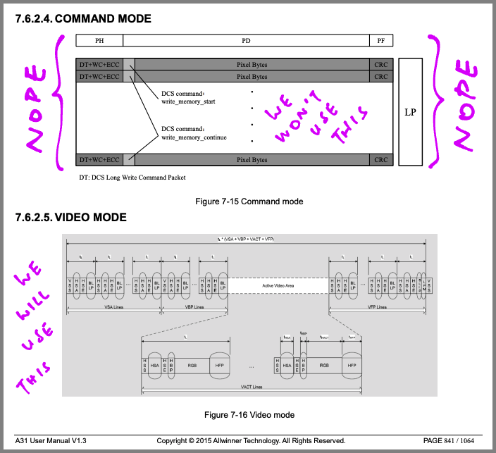
DSI Video Mode from A31 User Manual (Page 841)
What’s MIPI DSI Video Mode?
MIPI Display Serial Interface (DSI) supports 2 modes of operation (pic above)…
DSI Command Mode: For sending DCS Commands to the display
(DCS is the Display Command Set)
DSI Video Mode: For blasting pixels to the display
But the ST7703 Datasheet (page 19) says that DSI Command Mode is NOT supported…
ST7703 only support Video mode. Video Mode refers to operation in which transfers from the host processor to the peripheral take the form of a real-time pixel stream.
And while we’re in DSI Video Mode, PinePhone needs to pump pixels continuously to ST7703 (or the display goes blank)…
In normal operation, the driver IC relies on the host processor to provide image data at sufficient bandwidth to avoid flicker or other visible artifacts in the displayed image. Video information should only be transmitted using High Speed Mode.
So we’ll transmit our DCS Commands in DSI Video Mode? Even though it’s meant for blasting pixels?
Yeah earlier we talked about sending the DCS Long Write command for initialising PinePhone’s ST7703 LCD Controller…
We’ll have to transmit the command in DSI Video Mode. (Instead of DSI Command Mode)
It sounds odd, but that’s how ST7703 works!
Wait we’re mixing DCS Commands and Pixel Data in the same mode? Won’t ST7703 LCD Controller get confused?
If we flip back to the Display Command Set…
“Display Command Set for MIPI DSI”
(Also in the ST7703 Datasheet, page 34)
We see that the DCS Long Write command has a different Data Type (0x39) from the other Pixel Stream commands.
(Like “Packed Pixel Stream, 24-bit RGB, 8-8-8 Format”, Data Type 0x3E)
That’s why PinePhone’s Display doesn’t need a Data / Command Pin like PineTime.
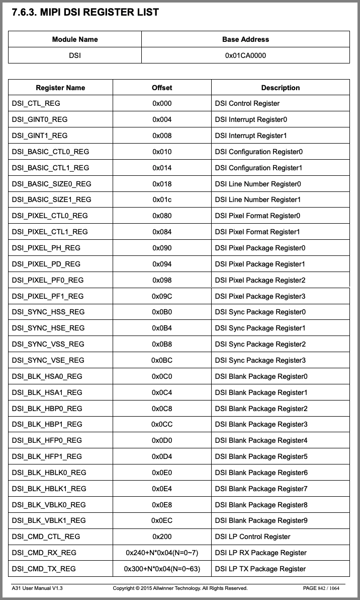
MIPI DSI Registers from A31 User Manual (Page 842)
How shall we send a DCS Long Write command to PinePhone’s Display?
To send a DCS Long Write command, we’ll set some Hardware Registers in A64’s MIPI DSI Controller.
The MIPI DSI Registers are missing from the A64 docs!
Yep it’s totally odd, but the A64 MIPI DSI Registers are actually documented in the Allwinner A31 SoC, which is a 32-bit SoC!
(A64 is actually an Allwinner H3 upgraded with 64-bit Arm Cores)
A64’s MIPI DSI Hardware is identical to A31 because both SoCs use the same MIPI DSI Driver…
static const struct of_device_id sun6i_dsi_of_table[] = {
  { .compatible = "allwinner,sun6i-a31-mipi-dsi" },
{ .compatible = "allwinner,sun50i-a64-mipi-dsi" },The Base Address of A64’s MIPI DSI Controller is 0x01CA 0000. (Pic above)
Also in the pic above is list of MIPI DSI Registers for A64 SoC.
For today we shall study 2 of the above registers…
DSI_BASIC_CTL1_REG (Offset 0x14)
DSI Configuration Register 1
DSI_CMD_TX_REG (Offset 0x300 to 0x3FC):
DSI Low Power Transmit Package Register
Though eventually we shall use these too…
DSI_CTL_REG (Offset 0x00)
DSI Control Register
DSI_BASIC_CTL0_REG (Offset 0x10)
DSI Configuration Register 0
DSI_CMD_CTL_REG (Offset 0x200)
DSI Low Power Control Register
DSI_CMD_RX_REG (Offset 0x240 to 0x25C)
DSI Low Power Receive Package Register
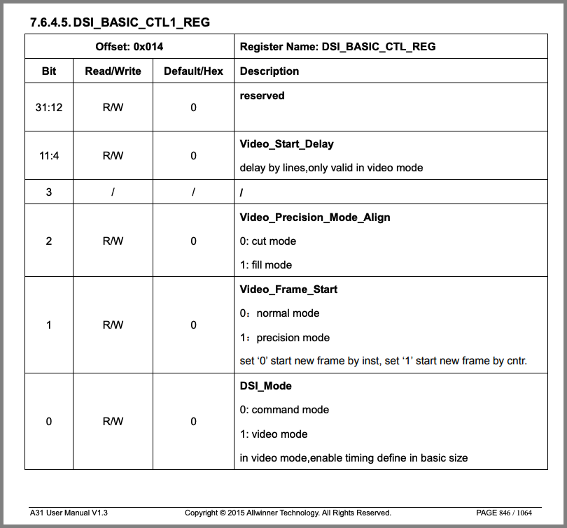
MIPI DSI Configuration Register 1 from A31 User Manual (Page 846)
We said earlier that PinePhone’s ST7789 LCD Controller needs to run in DSI Video Mode (instead of DSI Command Mode)…
At startup, our PinePhone Display Driver shall set DSI_Mode to 1. (Pic above)
That’s Bit 0 of DSI_BASIC_CTL1_REG (DSI Configuration Register 1) at Offset 0x14.
Our driver shall also set Video_Precision_Mode_Align to 1, Video_Frame_Start to 1 and Video_Start_Delay. (What’s the delay value?)
(Here’s how we set DSI_BASIC_CTL1_REG)
Anything else we should init at startup?
Actually we should turn on the MIPI DSI Controller BEFORE setting the Video Mode. At startup our driver shall set these registers…
DSI_CTL_REG (Offset 0x00):
Enable MIPI DSI (Bit 0)
DSI_BASIC_CTL0_REG (Offset 0x10):
Enable Error Correction Code (Bit 16)
Enable Cyclic Redundancy Check (Bit 17)
DSI_TRANS_START_REG (Offset 0x60, undocumented):
Set to 10 (Why?)
DSI_TRANS_ZERO_REG (Offset 0x78, undocumented):
Set to 0 (Why?)
DSI_DEBUG_DATA_REG (Offset 0x2f8, undocumented):
Set to 0xFF (Why?)
(Here’s how we set the registers)
Is that all?
There’s something else that needs to be initialised: MIPI DPHY, the Display Physical Layer for MIPI DSI.
Sadly A64’s MIPI DPHY doesn’t seem to be documented, so we might need to do Reverse Engineering. See this…
Don’t forget to switch on the Display Backlight!
Now that we have initialised A64 MIPI DSI, we’re ready to send our DCS Command…
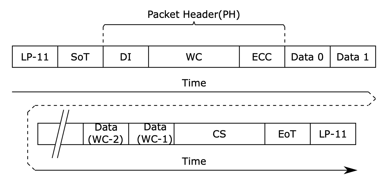
MIPI DSI Long Packet (Page 203)
Earlier we talked about transmitting a DCS Long Write command (Data Type 0x39) to ST7703 LCD Controller…
Page 32 of the ST7703 Datasheet says that we need to transmit a Long Packet in this format…
Packet Header (4 bytes):
Data Identifier (DI) (1 byte):
Virtual Channel Identifier (Bits 6 to 7)
Data Type (Bits 0 to 5)
Word Count (WC) (2 bytes):
Number of bytes in the Packet Payload
Error Correction Code (ECC) (1 byte):
Allow single-bit errors to be corrected and 2-bit errors to be detected in the Packet Header
Packet Payload:
Data (0 to 65,541 bytes):
Number of data bytes should match the Word Count (WC)
Packet Footer:
Checksum (CS) (2 bytes):
16-bit Cyclic Redundancy Check (CRC)
We have implemented MIPI DSI Long Packets in Apache NuttX Kernel…
Let’s program A64 to send this Long Packet.
(Page 32 of the ST7703 Datasheet also defines a Short Packet format, which is explained in the Appendix)
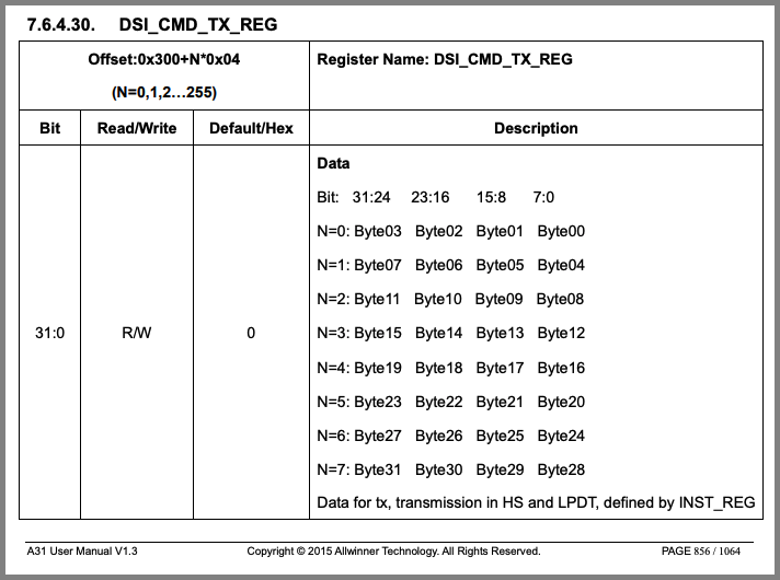
MIPI DSI Low Power Transmit Package Register from A31 User Manual (Page 856)
We’re finally ready to transmit the DCS Long Write command to ST7703 LCD Controller!
We begin by setting the following bits to 1 in DSI_CMD_CTL_REG (DSI Low Power Control Register) at Offset 0x200…
RX_Overflow (Bit 26): Clear flag for “Receive overflow”
RX_Flag (Bit 25): Clear flag for “Receive has started”
TX_Flag (Bit 9): Clear flag for “Transmit has started”
All other bits must be set to 0. (Like this)
We compose a Long Packet (or Short Packet) containing the DCS Long Write (or DCS Short Write) command…
The packet contains…
Packet Header
Packet Payload (only for Long Packet)
Packet Footer (only for Long Packet)
Now we write the packet to DSI_CMD_TX_REG (DSI Low Power Transmit Package Register) at Offset 0x300 to 0x3FC. (Pic above)
What’s N in the table above?
We may rewrite the table without N like so…
| Offset | Bits 31 to 24 | 23 to 16 | 15 to 8 | 7 to 0 |
|---|---|---|---|---|
0x300 | Byte 3 | Byte 2 | Byte 1 | Byte 0 |
0x304 | Byte 7 | Byte 6 | Byte 5 | Byte 4 |
0x308 | Byte 11 | Byte 10 | Byte 9 | Byte 8 |
| … |
Thus DSI_CMD_TX_REG works like a Packet Buffer that will contain the data to be transmitted over MIPI DSI.
Then we set Packet Length - 1 in Bits 0 to 7 (TX_Size) of DSI_CMD_CTL_REG (DSI Low Power Control Register) at Offset 0x200.
Finally we set DSI_INST_JUMP_SEL_REG (Offset 0x48, undocumented) to begin the Low Power Transmission.
(How we write the packet to DSI_CMD_TX_REG)
We also need to…
Disable DSI Processing:
Set Instru_En to 0 (Like this)
Then Enable DSI Processing:
Set Instru_En to 1 (Like this)
Instru_En is Bit 0 of DSI_BASIC_CTL0_REG (DSI Configuration Register 0) at Offset 0x10.
How will we know when the transmission is complete?
To check whether the transmission is complete, we poll on Instru_En.
Wow this looks super complicated!
Yeah. The complete steps to initialise the ST7703 LCD Controller will look like this…
We have implemented the sending of MIPI DSI Packets in Apache NuttX Kernel…
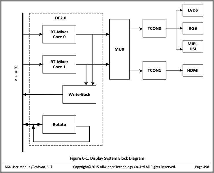
Display Engine (DE) and Timing Controller (TCON0) from A64 User Manual (Page 498)
OK we have initialised the ST7703 display…
What about rendering the display?
Remember we said that the ST7703 LCD Controller is RAM-less? And thus we need to pump a constant stream of pixels to the display?
To do this, we program two controllers in Allwinner A64…
Display Engine (DE): Execute the Rendering Pipeline to generate the pixels for display
(Handles image buffering, scaling, mixing, …)
Timing Controller (TCON0): Pump the generated pixels at the right clock frequency to the MIPI DSI display
(Pic above)
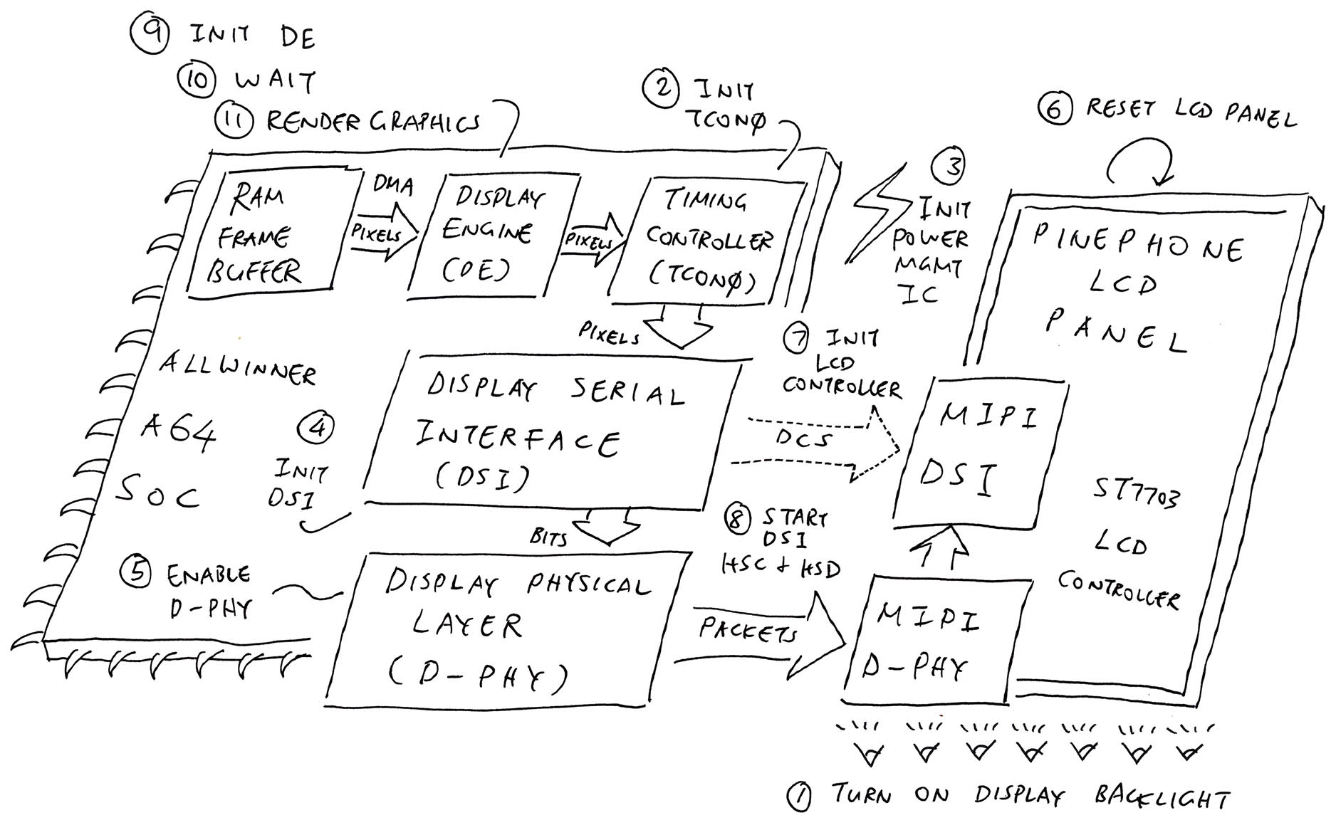
Is there a specific sequence of steps for calling the Display Serial Interface, Display Engine and Timing Controller?
To render graphics on PinePhone’s LCD Display, our Display Driver needs to follow these steps…
We’ll explain all these in the next article!
u/immibis on Reddit has shared some helpful tips…
“To actually display pixels on the screen you also need to program DE and TCON. I saw something somewhere about a test pattern that might be able to bypass this, and a framebuffer mode that bypasses the mixing IIRC.”
And we might hit some undocumented A64 Registers…
“several important registers used by the driver aren’t documented (the command registers) but the basic format is shown in the driver source code”
“…the module is running a little instruction set and the manual conspicuously omits any description of the instructions or even the registers where you put the instructions.”
We’ll find out soon in the next article!
Apache NuttX RTOS booting on PinePhone
Once again, why are we doing all this?
We’re now porting Apache NuttX RTOS to PinePhone.
But it will look awfully dull until we render something on PinePhone’s LCD Display!
That’s why we’re probing the internals of PinePhone to create a NuttX Display Driver.
How shall we build the NuttX Driver for PinePhone’s Display?
Our NuttX Display Driver for PinePhone shall implement these functions (pic below)…
We have completed the Zig Implementation of the NuttX Driver…
We’re porting the Zig Driver to C and adding to NuttX Kernel…
Stay Tuned for Updates!
Inside our Complete Display Driver for PinePhone
I hope we learnt lots about PinePhone’s Display…
What’s a MIPI Display Serial Interface (DSI)
What’s inside PinePhone’s LCD Display
How it’s similar to PineTime’s Display Controller
Implications of a RAM-less Display Controller
What are PinePhone’s Display Engine (DE) and Timing Controller (TCON)
Please join me in the next article when we’ll build a PinePhone Display Driver in Zig!
Please check out the other articles on NuttX for PinePhone…
Many Thanks to my GitHub Sponsors for supporting my work! This article wouldn’t have been possible without your support.
Got a question, comment or suggestion? Create an Issue or submit a Pull Request here…
All writes to MIPI DSI Hardware Registers must use Data Memory Barrier (DMB)
How did we find the Reference Code for the MIPI DSI Driver? We used GitHub Code Search…
This doc explains MIPI DSI rather well…
(Page 181, Chapter 12: “DSI”)
ST7703 always runs in DSI Video Mode (instead of Command Mode).
Does this mean that all DCS Commands are sent over all 4 DSI Data Lanes? (Instead of DSI Lane 0 only)
UPDATE: At Startup, DCS Commands are sent over DSI Lane 0. After Startup, Pixel Data is sent over Multiple DSI Data Lanes in Video Mode. Which means the Pixel Data is pushed as a continuous stream of Video Pixels, instead of plotting every pixel command by command.
Can we receive data from ST7703?
Inside our Complete Display Driver for PinePhone
Is there a specific sequence of steps for calling the Display Serial Interface, Display Engine and Timing Controller?
To render graphics on PinePhone’s LCD Display, our Display Driver needs to follow these steps: render.zig
Turn on Display Backlight
Initialise Timing Controller (TCON0)
Initialise Power Management Integrated Circuit (PMIC) and wait 15 milliseconds
Enable MIPI DSI Block
Enable MIPI Display Physical Layer (DPHY)
Reset LCD Panel and wait 15 milliseconds
Initialise LCD Controller (ST7703)
Start MIPI DSI HSC and HSD
(High Speed Clock Mode and High Speed Data Transmission)
Initialise Display Engine (DE)
Wait 160 milliseconds
Render Graphics with Display Engine (DE)
Earlier we talked about the sequence of steps that our Display Driver needs to follow…
This section explains how we enable the Allwinner A64 MIPI DSI Block, before calling it to transmit MIPI DSI Commands to the ST7703 LCD Controller.
We captured the log from p-boot dsi_init…
By decoding the captured addresses and values, we decipher the following steps to enable the Allwinner A64 MIPI DSI Block…
Enable MIPI DSI Bus
BUS_CLK_GATING_REG0: CCU Offset 0x60 (A64 Page 100)
BUS_SOFT_RST_REG0: CCU Offset 0x2C0 (A64 Page 138)
CCU Base Address: 0x01C2 0000 (A64 Page 82)
mipi dsi bus enable
setbits 0x1c20060, 0x2 (DMB)
setbits 0x1c202c0, 0x2 (DMB)
Enable DSI Block
DSI_CTL_REG: DSI Offset 0x0 (A31 Page 843)
DSI_BASIC_CTL0_REG: DSI Offset 0x10 (A31 Page 845)
DSI_TRANS_START_REG: DSI Offset 0x60 (Undocumented)
DSI_TRANS_ZERO_REG: DSI Offset 0x78 (Undocumented)
DSI Base Address: 0x01CA 0000 (A31 Page 842)
Enable the DSI block
0x1ca0000 = 0x1 (DMB)
0x1ca0010 = 0x30000 (DMB)
0x1ca0060 = 0xa (DMB)
0x1ca0078 = 0x0 (DMB)
Set Instructions (Undocumented)
DSI_INST_FUNC_REG(0): DSI Offset 0x20
0x1fDSI_INST_FUNC_REG(1): DSI Offset 0x24
0x1000 0001DSI_INST_FUNC_REG(2): DSI Offset 0x28
0x2000 0010DSI_INST_FUNC_REG(3): DSI Offset 0x2c
0x2000 000fDSI_INST_FUNC_REG(4): DSI Offset 0x30
0x3010 0001DSI_INST_FUNC_REG(5): DSI Offset 0x34
0x4000 0010DSI_INST_FUNC_REG(6): DSI Offset 0x38
0xfDSI_INST_FUNC_REG(7): DSI Offset 0x3c
0x5000 001f(DSI_INST_FUNC_REG(n) is (0x020 + (n) * 0x04))
inst_init
0x1ca0020 = 0x1f (DMB)
0x1ca0024 = 0x10000001 (DMB)
0x1ca0028 = 0x20000010 (DMB)
0x1ca002c = 0x2000000f (DMB)
0x1ca0030 = 0x30100001 (DMB)
0x1ca0034 = 0x40000010 (DMB)
0x1ca0038 = 0xf (DMB)
0x1ca003c = 0x5000001f (DMB)
Configure Jump Instructions (Undocumented)
DSI_INST_JUMP_CFG_REG(0): DSI Offset 0x4c
0x56 0001(DSI_INST_JUMP_CFG_REG(n) is (0x04c + (n) * 0x04))
DSI_DEBUG_DATA_REG: DSI Offset 0x2f8
0xff0x1ca004c = 0x560001 (DMB)
0x1ca02f8 = 0xff (DMB)Set Video Start Delay
DSI_BASIC_CTL1_REG: DSI Offset 0x14 (A31 Page 846)
Note: Video_Start_Delay is actually 13 bits, not 8 bits as stated in the A31 User Manual
get_video_start_delay
0x1ca0014 = 0x5bc7 (DMB)
Set Burst (Undocumented)
DSI_TCON_DRQ_REG: DSI Offset 0x7c
0x1000 0007setup_burst
0x1ca007c = 0x10000007 (DMB)Set Instruction Loop (Undocumented)
DSI_INST_LOOP_SEL_REG: DSI Offset 0x40
0x3000 0002DSI_INST_LOOP_NUM_REG(0): DSI Offset 0x44
0x31 0031DSI_INST_LOOP_NUM_REG(1): DSI Offset 0x54
0x31 0031(DSI_INST_LOOP_NUM_REG(n) is (0x044 + (n) * 0x10))
setup_inst_loop
0x1ca0040 = 0x30000002 (DMB)
0x1ca0044 = 0x310031 (DMB)
0x1ca0054 = 0x310031 (DMB)
Set Pixel Format
DSI_PIXEL_PH_REG: DSI Offset 0x90 (A31 Page 848)
0x3E (24-bit Video Mode)DSI_PIXEL_PF0_REG: DSI Offset 0x98 (A31 Page 849)
0xffff (Force CRC to this value)DSI_PIXEL_PF1_REG: DSI Offset 0x9c (A31 Page 849)
0xffff (CRC initial to this value in transmitions except 1st one)0xffff (CRC initial to this value in 1st transmition every frame)DSI_PIXEL_CTL0_REG: DSI Offset 0x80 (A31 Page 847)
setup_format
0x1ca0090 = 0x1308703e (DMB)
0x1ca0098 = 0xffff (DMB)
0x1ca009c = 0xffffffff (DMB)
0x1ca0080 = 0x10008 (DMB)
Set Sync Timings
DSI_BASIC_CTL_REG: DSI Offset 0x0c (Undocumented)
DSI_SYNC_HSS_REG: DSI Offset 0xb0 (A31 Page 850)
0x120x21 (HSS)DSI_SYNC_HSE_REG: DSI Offset 0xb4 (A31 Page 850)
0x31 (HSE)DSI_SYNC_VSS_REG: DSI Offset 0xb8 (A31 Page 851)
DSI_SYNC_VSE_REG: DSI Offset 0xbc (A31 Page 851)
0x140x11 (VSE)setup_timings
0x1ca000c = 0x0 (DMB)
0x1ca00b0 = 0x12000021 (DMB)
0x1ca00b4 = 0x1000031 (DMB)
0x1ca00b8 = 0x7000001 (DMB)
0x1ca00bc = 0x14000011 (DMB)Set Basic Size (Undocumented)
DSI_BASIC_SIZE0_REG: DSI Offset 0x18
DSI_BASIC_SIZE1_REG: DSI Offset 0x1c
0x1ca0018 = 0x11000a (DMB)
0x1ca001c = 0x5cd05a0 (DMB)
Set Horizontal Blanking
DSI_BLK_HSA0_REG: DSI Offset 0xc0 (A31 Page 852)
0x900 4a19DSI_BLK_HSA1_REG: DSI Offset 0xc4 (A31 Page 852)
0x50b4DSI_BLK_HBP0_REG: DSI Offset 0xc8 (A31 Page 852)
0x3500 5419DSI_BLK_HBP1_REG: DSI Offset 0xcc (A31 Page 852)
0x757aDSI_BLK_HFP0_REG: DSI Offset 0xd0 (A31 Page 852)
0x900 4a19DSI_BLK_HFP1_REG: DSI Offset 0xd4 (A31 Page 853)
0x50b4DSI_BLK_HBLK0_REG: DSI Offset 0xe0 (A31 Page 853)
0xc09 1a19DSI_BLK_HBLK1_REG: DSI Offset 0xe4 (A31 Page 853)
0x72bd0x1ca00c0 = 0x9004a19 (DMB)
0x1ca00c4 = 0x50b40000 (DMB)
0x1ca00c8 = 0x35005419 (DMB)
0x1ca00cc = 0x757a0000 (DMB)
0x1ca00d0 = 0x9004a19 (DMB)
0x1ca00d4 = 0x50b40000 (DMB)
0x1ca00e0 = 0xc091a19 (DMB)
0x1ca00e4 = 0x72bd0000 (DMB)Set Vertical Blanking
DSI_BLK_VBLK0_REG: DSI Offset 0xe8 (A31 Page 854)
0x1a00 0019DSI_BLK_VBLK1_REG: DSI Offset 0xec (A31 Page 854)
0xffff0x1ca00e8 = 0x1a000019 (DMB)
0x1ca00ec = 0xffff0000 (DMB)Based on the above steps, we have implemented in Zig the PinePhone Driver that enables the Allwinner A64 MIPI DSI Block…
We have implemented the driver in Apache NuttX Kernel…
Earlier we talked about the sequence of steps that our Display Driver needs to follow…
This section explains how we start Allwinner A64 MIPI DSI in HSC and HSD Modes, before calling it to transmit MIPI DSI Commands to the ST7703 LCD Controller.
(High Speed Clock Mode and High Speed Data Transmission)
We captured the log from p-boot dsi_init…
By decoding the captured addresses and values, we decipher the following steps to start Allwinner A64 MIPI DSI in HSC and HSD Modes…
Start HSC (Undocumented)
DSI_INST_JUMP_SEL_REG: DSI Offset 0x48
0xf02DSI Base Address: 0x01CA 0000 (A31 Page 842)
dsi_start DSI_START_HSC
0x1ca0048 = 0xf02 (DMB)
Commit
DSI_BASIC_CTL0_REG: DSI Offset 0x10 (A31 Page 845)
dsi_update_bits: 0x01ca0010 : 00030000 -> (00000001) 00000001 (DMB)
addr=0x1ca0010, mask=0x1, val=0x1 (DMB)
Instruction Function Lane (Undocumented)
DSI_INST_FUNC_REG(0): DSI Offset 0x20
(DSI_INST_FUNC_REG(n) is (0x020 + (n) * 0x04))
dsi_update_bits: 0x01ca0020 : 0000001f -> (00000010) 00000000 (DMB)
addr=0x1ca0020, mask=0x10, val=0x0 (DMB)
Wait 1,000 microseconds
udelay 1000Start HSD (Undocumented)
DSI_INST_JUMP_SEL_REG: DSI Offset 0x48
0x63f0 7006dsi_start DSI_START_HSD
0x1ca0048 = 0x63f07006 (DMB)Commit
DSI_BASIC_CTL0_REG: DSI Offset 0x10 (A31 Page 845)
dsi_update_bits: 0x01ca0010 : 00030000 -> (00000001) 00000001 (DMB)
addr=0x1ca0010, mask=0x1, val=0x1 (DMB)
Based on the above steps, we have implemented in Zig the PinePhone Driver that starts Allwinner A64 MIPI DSI (in HSC and HSD Modes)…
We have implemented the driver in Apache NuttX Kernel…
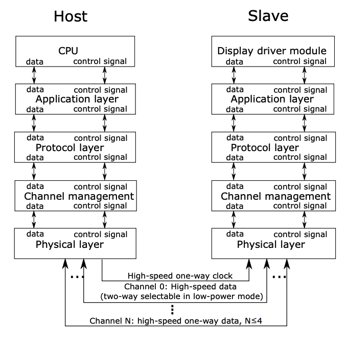
MIPI DSI Protocol Layers (Page 183)
Earlier we talked about initialising the MIPI DSI Controller…
There’s something else that needs to be initialised: MIPI DPHY, the Display Physical Layer for MIPI DSI…
MIPI DPHY is the “Physical Layer” in the pic above.
(MIPI DSI runs in the layers above MIPI DPHY)
Sadly Allwinner A64’s MIPI DPHY doesn’t seem to be documented, so we might need to do Reverse Engineering.
How do we implement MIPI DPHY if it’s undocumented?
We captured the log from p-boot dphy_enable…
By decoding the captured addresses and values, we decipher the following steps to enable the Allwinner A64 MIPI Display Physical Layer (DPHY)…
Set DSI Clock to 150 MHz (600 MHz / 4)
MIPI_DSI_CLK_REG: CCU Offset 0x168 (A64 Page 122)
0b10 (DSI DPHY Clock Source is PLL_PERIPH0(1X))CCU Base Address: 0x01C2 0000 (A64 Page 82)
150MHz (600 / 4)
0x1c20168 = 0x8203 (DMB)
Power on DPHY Tx (Undocumented)
DPHY_TX_CTL_REG: DPHY Offset 0x04
0x1000 0000DPHY_TX_TIME0_REG: DPHY Offset 0x10
0xa06 000eDPHY_TX_TIME1_REG: DPHY Offset 0x14
0xa03 3207DPHY_TX_TIME2_REG: DPHY Offset 0x18
0x1eDPHY_TX_TIME3_REG: DPHY Offset 0x1c
0x0DPHY_TX_TIME4_REG: DPHY Offset 0x20
0x303DPHY Base Address: 0x01ca 1000
0x1ca1004 = 0x10000000 (DMB)
0x1ca1010 = 0xa06000e (DMB)
0x1ca1014 = 0xa033207 (DMB)
0x1ca1018 = 0x1e (DMB)
0x1ca101c = 0x0 (DMB)
0x1ca1020 = 0x303 (DMB)
Enable DPHY (Undocumented)
DPHY_GCTL_REG: DPHY Offset 0x00 (Enable DPHY)
0x31DPHY_ANA0_REG: DPHY Offset 0x4c (PWS)
0x9f00 7f00DPHY_ANA1_REG: DPHY Offset 0x50 (CSMPS)
0x1700 0000DPHY_ANA4_REG: DPHY Offset 0x5c (CKDV)
0x1f0 1555DPHY_ANA2_REG: DPHY Offset 0x54 (ENIB)
0x2Wait 5 microseconds
0x1ca1000 = 0x31 (DMB)
0x1ca104c = 0x9f007f00 (DMB)
0x1ca1050 = 0x17000000 (DMB)
0x1ca105c = 0x1f01555 (DMB)
0x1ca1054 = 0x2 (DMB)
udelay 5
Enable LDOR, LDOC, LDOD (Undocumented)
DPHY_ANA3_REG: DPHY Offset 0x58 (Enable LDOR, LDOC, LDOD)
0x304 0000Wait 1 microsecond
DPHY_ANA3_REG: DPHY Offset 0x58 (Enable VTTC, VTTD)
0xf800 0000Wait 1 microsecond
DPHY_ANA3_REG: DPHY Offset 0x58 (Enable DIV)
0x400 0000Wait 1 microsecond
DPHY_ANA2_REG: DPHY Offset 0x54 (Enable CK_CPU)
0x10Wait 1 microsecond
DPHY_ANA1_REG: DPHY Offset 0x50 (VTT Mode)
0x8000 0000DPHY_ANA2_REG: DPHY Offset 0x54 (Enable P2S CPU)
0xf00 00000x1ca1058 = 0x3040000 (DMB)
udelay 1
update_bits addr=0x1ca1058, mask=0xf8000000, val=0xf8000000 (DMB)
udelay 1
update_bits addr=0x1ca1058, mask=0x4000000, val=0x4000000 (DMB)
udelay 1
update_bits addr=0x1ca1054, mask=0x10, val=0x10 (DMB)
udelay 1
update_bits addr=0x1ca1050, mask=0x80000000, val=0x80000000 (DMB)
update_bits addr=0x1ca1054, mask=0xf000000, val=0xf000000 (DMB)Based on the above steps, we have implemented in Zig the PinePhone Driver that enables the Allwinner A64 MIPI Display Physical Layer (DPHY)…
We have implemented the driver in Apache NuttX Kernel…
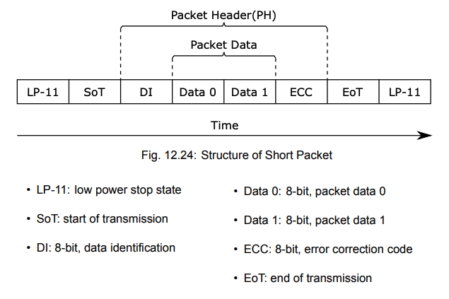
MIPI DSI Short Packet (Page 201)
According to BL808 Reference Manual (Page 201, pic above)…
A Short Packet consists of 8-bit data identification (DI), two bytes of commands or data, and 8-bit ECC.
The length of a short packet is 4 bytes including ECC.
Thus a MIPI DSI Short Packet (compared with Long Packet)…
Doesn’t have Packet Payload and Packet Footer (CRC)
Instead of Word Count (WC), the Packet Header now has 2 bytes of data
DCS Command (Data Type) is…
DCS Short Write Without Parameter (0x05) for sending 1 byte of data
DCS Short Write With Parameter (0x15) for sending 2 bytes of data
Everything else is the same.
We have implemented MIPI DSI Short Packets in Apache NuttX Kernel…
Earlier we talked about the sequence of steps that our Display Driver needs to follow…
Xingbangda has provided an Initialisation Sequence of (magical) ST7703 Commands that we should send to the LCD Controller at startup.
The commands below are (mostly) documented in the ST7703 Datasheet…
The Initialisation Sequence consists of the following 20 DCS Commands that we should send via DCS Short Write or DCS Long Write…
| Byte | Purpose |
|---|---|
| #1 | |
0xB9 | SETEXTC (Page 131): Enable USER Command |
0xF1 | Enable User command |
0x12 | (Continued) |
0x83 | (Continued) |
|
| #2
| 0xBA | SETMIPI (Page 144):
Set MIPI related register
| 0x33 | Virtual Channel = 0
(VC_Main = 0)
Number of Lanes = 4
(Lane_Number = 3)
| 0x81 | LDO = 1.7 V
(DSI_LDO_SEL = 4)
Terminal Resistance = 90 Ohm
(RTERM = 1)
| 0x05 | MIPI Low High Speed driving ability = x6
(IHSRX = 5)
| 0xF9 | TXCLK speed in DSI LP mode = fDSICLK / 16
(Tx_clk_sel = 2)
| 0x0E | Min HFP number in DSI mode = 14
(HFP_OSC = 14)
| 0x0E | Min HBP number in DSI mode = 14
(HBP_OSC = 14)
| 0x20 | Undocumented
| 0x00 | Undocumented
| 0x00 | Undocumented
| 0x00 | Undocumented
| 0x00 | Undocumented
| 0x00 | Undocumented
| 0x00 | Undocumented
| 0x00 | Undocumented
| 0x44 | Undocumented
| 0x25 | Undocumented
| 0x00 | Undocumented
| 0x91 | Undocumented
| 0x0a | Undocumented
| 0x00 | Undocumented
| 0x00 | Undocumented
| 0x02 | Undocumented
| 0x4F | Undocumented
| 0x11 | Undocumented
| 0x00 | Undocumented
| 0x00 | Undocumented
| 0x37 | Undocumented
|
| #3
| 0xB8 | SETPOWER_EXT (Page 142):
Set display related register
| 0x25 | External power IC or PFM: VSP = FL1002, VSN = FL1002
(PCCS = 2)
VCSW1 / VCSW2 Frequency for Pumping VSP / VSN = 1/4 Hsync
(ECP_DC_DIV = 5)
| 0x22 | VCSW1/VCSW2 soft start time = 15 ms
(DT = 2)
Pumping ratio of VSP / VSN with VCI = x2
(XDK_ECP = 1)
| 0x20 | PFM operation frequency FoscD = Fosc/1
(PFM_DC_DIV = 0)
| 0x03 | Enable power IC pumping frequency synchronization = Synchronize with external Hsync
(ECP_SYNC_EN = 1)
Enable VGH/VGL pumping frequency synchronization = Synchronize with external Hsync
(VGX_SYNC_EN = 1)
|
| #4
| 0xB3 | SETRGBIF (Page 134):
Control RGB I/F porch timing for internal use
| 0x10 | Vertical back porch HS number in Blank Frame Period = Hsync number 16
(VBP_RGB_GEN = 16)
| 0x10 | Vertical front porch HS number in Blank Frame Period = Hsync number 16
(VFP_RGB_GEN = 16)
| 0x05 | HBP OSC number in Blank Frame Period = OSC number 5
(DE_BP_RGB_GEN = 5)
| 0x05 | HFP OSC number in Blank Frame Period = OSC number 5
(DE_FP_RGB_GEN = 5)
| 0x03 | Undocumented
| 0xFF | Undocumented
| 0x00 | Undocumented
| 0x00 | Undocumented
| 0x00 | Undocumented
| 0x00 | Undocumented
|
| #5
| 0xC0 | SETSCR (Page 147):
Set related setting of Source driving
| 0x73 | Source OP Amp driving period for positive polarity in Normal Mode: Source OP Period = 1154/Fosc
(N_POPON = 115)
| 0x73 | Source OP Amp driving period for negative polarity in Normal Mode: Source OP Period = 1154/Fosc
(N_NOPON = 115)
| 0x50 | Source OP Amp driving period for positive polarity in Idle mode: Source OP Period = 804/Fosc
(I_POPON = 80)
| 0x50 | Source OP Amp dirivng period for negative polarity in Idle Mode: Source OP Period = 804/Fosc
(I_NOPON = 80)
| 0x00 | (SCR Bits 24-31 = 0x00)
| 0xC0 | (SCR Bits 16-23 = 0xC0)
| 0x08 | Gamma bias current fine tune: Current xIbias = 4
(SCR Bits 9-13 = 4)
(SCR Bits 8-15 = 0x08)
| 0x70 | Source and Gamma bias current core tune: Ibias = 1
(SCR Bits 0-3 = 0)
Source bias current fine tune: Current xIbias = 7
(SCR Bits 4-8 = 7)
(SCR Bits 0-7 = 0x70)
| 0x00 | Undocumented
|
| #6
| 0xBC | SETVDC (Page 146):
Control NVDDD/VDDD Voltage
| 0x4E | NVDDD voltage = -1.8 V
(NVDDD_SEL = 4)
VDDD voltage = 1.9 V
(VDDD_SEL = 6)
|
| #7
| 0xCC | SETPANEL (Page 154):
Set display related register
| 0x0B | Enable reverse the source scan direction
(SS_PANEL = 1)
Normal vertical scan direction
(GS_PANEL = 0)
Normally black panel
(REV_PANEL = 1)
S1:S2:S3 = B:G:R
(BGR_PANEL = 1)
|
| #8
| 0xB4 | SETCYC (Page 135):
Control display inversion type
| 0x80 | Extra source for Zig-Zag Inversion = S2401
(ZINV_S2401_EN = 1)
Row source data dislocates = Even row
(ZINV_G_EVEN_EN = 0)
Disable Zig-Zag Inversion
(ZINV_EN = 0)
Enable Zig-Zag1 Inversion
(ZINV2_EN = 0)
Normal mode inversion type = Column inversion
(N_NW = 0)
|
| #9
| 0xB2 | SETDISP (Page 132):
Control the display resolution
| 0xF0 | Gate number of vertical direction = 480 +
(240*4)
(NL = 240)
| 0x12 | (RES_V_LSB = 0)
Non-display area source output control: Source output = VSSD
(BLK_CON = 1)
Channel number of source direction = 720RGB
(RESO_SEL = 2)
| 0xF0 | Source voltage during Blanking Time when accessing Sleep-Out / Sleep-In = GND
(WHITE_GND_EN = 1)
Blank timing control when access sleep out command: Blank Frame Period = 7 Frames
(WHITE_FRAME_SEL = 7)
Source output refresh control: Refresh Period = 0 Frames
(ISC = 0)
|
| #10
| 0xE3 | SETEQ (Page 159):
Set EQ related register
| 0x00 | Temporal spacing between HSYNC and PEQGND = 04/Fosc
(PNOEQ = 0)
| 0x00 | Temporal spacing between HSYNC and NEQGND = 04/Fosc
(NNOEQ = 0)
| 0x0B | Source EQ GND period when Source up to positive voltage = 114/Fosc
(PEQGND = 11)
| 0x0B | Source EQ GND period when Source down to negative voltage = 114/Fosc
(NEQGND = 11)
| 0x10 | Source EQ VCI period when Source up to positive voltage = 164/Fosc
(PEQVCI = 16)
| 0x10 | Source EQ VCI period when Source down to negative voltage = 164/Fosc
(NEQVCI = 16)
| 0x00 | Temporal period of PEQVCI1 = 04/Fosc
(PEQVCI1 = 0)
| 0x00 | Temporal period of NEQVCI1 = 04/Fosc
(NEQVCI1 = 0)
| 0x00 | (Reserved)
| 0x00 | (Reserved)
| 0xFF | (Undocumented)
| 0x00 | (Reserved)
| 0xC0 | White pattern to protect GOA glass
(ESD_DET_DATA_WHITE = 1)
Enable ESD detection function to protect GOA glass
(ESD_WHITE_EN = 1)
| 0x10 | No Need VSYNC
(additional frame) after Sleep-In to display sleep-in blanking frame then into Sleep-In State
(SLPIN_OPTION = 1)
Enable video function detection
(VEDIO_NO_CHECK_EN = 0)
Disable ESD white pattern scanning voltage pull ground
(ESD_WHITE_GND_EN = 0)
ESD detection function period = 0 Frames
(ESD_DET_TIME_SEL = 0)
|
| #11
| 0xC6 | Undocumented
| 0x01 | Undocumented
| 0x00 | Undocumented
| 0xFF | Undocumented
| 0xFF | Undocumented
| 0x00 | Undocumented
|
| #12
| 0xC1 | SETPOWER (Page 149):
Set related setting of power
| 0x74 | VGH Voltage Adjustment = 17 V
(VBTHS = 7)
VGL Voltage Adjustment = -11 V
(VBTLS = 4)
| 0x00 | Enable VGH feedback voltage detection. Output voltage = VBTHS
(FBOFF_VGH = 0)
Enable VGL feedback voltage detection. Output voltage = VBTLS
(FBOFF_VGL = 0)
| 0x32 | VSPROUT Voltage =
(VRH[5:0] x 0.05 + 3.3) x
(VREF/4.8) if VREF [4]=0
(VRP = 50)
| 0x32 | VSNROUT Voltage =
(VRH[5:0] x 0.05 + 3.3) x
(VREF/5.6) if VREF [4]=1
(VRN = 50)
| 0x77 | Undocumented
| 0xF1 | Enable VGL voltage Detect Function = VGL voltage Abnormal
(VGL_DET_EN = 1)
Enable VGH voltage Detect Function = VGH voltage Abnormal
(VGH_DET_EN = 1)
Enlarge VGL Voltage at “FBOFF_VGL=1” = “VGL=-15V”
(VGL_TURBO = 1)
Enlarge VGH Voltage at “FBOFF_VGH=1” = “VGH=20V”
(VGH_TURBO = 1)
(APS = 1)
| 0xFF | Left side VGH stage 1 pumping frequency = 1.5 MHz
(VGH1_L_DIV = 15)
Left side VGL stage 1 pumping frequency = 1.5 MHz
(VGL1_L_DIV = 15)
| 0xFF | Right side VGH stage 1 pumping frequency = 1.5 MHz
(VGH1_R_DIV = 15)
Right side VGL stage 1 pumping frequency = 1.5 MHz
(VGL1_R_DIV = 15)
| 0xCC | Left side VGH stage 2 pumping frequency = 2.6 MHz
(VGH2_L_DIV = 12)
Left side VGL stage 2 pumping frequency = 2.6 MHz
(VGL2_L_DIV = 12)
| 0xCC | Right side VGH stage 2 pumping frequency = 2.6 MHz
(VGH2_R_DIV = 12)
Right side VGL stage 2 pumping frequency = 2.6 MHz
(VGL2_R_DIV = 12)
| 0x77 | Left side VGH stage 3 pumping frequency = 4.5 MHz
(VGH3_L_DIV = 7)
Left side VGL stage 3 pumping frequency = 4.5 MHz
(VGL3_L_DIV = 7)
| 0x77 | Right side VGH stage 3 pumping frequency = 4.5 MHz
(VGH3_R_DIV = 7)
Right side VGL stage 3 pumping frequency = 4.5 MHz
(VGL3_R_DIV = 7)
|
| #13
| 0xB5 | SETBGP (Page 136):
Internal reference voltage setting
| 0x07 | VREF Voltage: 4.2 V
(VREF_SEL = 7)
| 0x07 | NVREF Voltage: 4.2 V
(NVREF_SEL = 7)
|
| #14
| 0xB6 | SETVCOM (Page 137):
Set VCOM Voltage
| 0x2C | VCOMDC voltage at “GS_PANEL=0” = -0.67 V
(VCOMDC_F = 0x2C)
| 0x2C | VCOMDC voltage at “GS_PANEL=1” = -0.67 V
(VCOMDC_B = 0x2C)
|
| #15
| 0xBF | Undocumented
| 0x02 | Undocumented
| 0x11 | Undocumented
| 0x00 | Undocumented
|
| #16
| 0xE9 | SETGIP1 (Page 163):
Set forward GIP timing
| 0x82 | SHR0, SHR1, CHR, CHR2 refer to Internal DE
(REF_EN = 1)
(PANEL_SEL = 2)
| 0x10 | Starting position of GIP STV group 0 = 4102 HSYNC
(SHR0 Bits 8-12 = 0x10)
| 0x06 | (SHR0 Bits 0-7 = 0x06)
| 0x05 | Starting position of GIP STV group 1 = 1442 HSYNC
(SHR1 Bits 8-12 = 0x05)
| 0xA2 | (SHR1 Bits 0-7 = 0xA2)
| 0x0A | Distance of STV rising edge and HYSNC = 102 Fosc
(SPON Bits 0-7 = 0x0A)
| 0xA5 | Distance of STV falling edge and HYSNC = 1652 Fosc
(SPOFF Bits 0-7 = 0xA5)
| 0x12 | STV0_1 distance with STV0_0 = 1 HSYNC
(SHR0_1 = 1)
STV0_2 distance with STV0_0 = 2 HSYNC
(SHR0_2 = 2)
| 0x31 | STV0_3 distance with STV0_0 = 3 HSYNC
(SHR0_3 = 3)
STV1_1 distance with STV1_0 = 1 HSYNC
(SHR1_1 = 1)
| 0x23 | STV1_2 distance with STV1_0 = 2 HSYNC
(SHR1_2 = 2)
STV1_3 distance with STV1_0 = 3 HSYNC
(SHR1_3 = 3)
| 0x37 | STV signal high pulse width = 3 HSYNC
(SHP = 3)
Total number of STV signal = 7
(SCP = 7)
| 0x83 | Starting position of GIP CKV group 0
(CKV0_0) = 131 HSYNC
(CHR = 0x83)
| 0x04 | Distance of CKV rising edge and HYSNC = 42 Fosc
(CON Bits 0-7 = 0x04)
| 0xBC | Distance of CKV falling edge and HYSNC = 1882 Fosc
(COFF Bits 0-7 = 0xBC)
| 0x27 | CKV signal high pulse width = 2 HSYNC
(CHP = 2)
Total period cycle of CKV signal = 7 HSYNC
(CCP = 7)
| 0x38 | Extra gate counter at blanking area: Gate number = 56
(USER_GIP_GATE = 0x38)
| 0x0C | Left side GIP output pad signal = ???
(CGTS_L Bits 16-21 = 0x0C)
| 0x00 | (CGTS_L Bits 8-15 = 0x00)
| 0x03 | (CGTS_L Bits 0-7 = 0x03)
| 0x00 | Normal polarity of Left side GIP output pad signal
(CGTS_INV_L Bits 16-21 = 0x00)
| 0x00 | (CGTS_INV_L Bits 8-15 = 0x00)
| 0x00 | (CGTS_INV_L Bits 0-7 = 0x00)
| 0x0C | Right side GIP output pad signal = ???
(CGTS_R Bits 16-21 = 0x0C)
| 0x00 | (CGTS_R Bits 8-15 = 0x00)
| 0x03 | (CGTS_R Bits 0-7 = 0x03)
| 0x00 | Normal polarity of Right side GIP output pad signal
(CGTS_INV_R Bits 16-21 = 0x00)
| 0x00 | (CGTS_INV_R Bits 8-15 = 0x00)
| 0x00 | (CGTS_INV_R Bits 0-7 = 0x00)
| 0x75 | Left side GIP output pad signal = ???
(COS1_L = 7)
Left side GIP output pad signal = ???
(COS2_L = 5)
| 0x75 | Left side GIP output pad signal = ???
(COS3_L = 7)
(COS4_L = 5)
| 0x31 | Left side GIP output pad signal = ???
(COS5_L = 3)
(COS6_L = 1)
| 0x88 | Reserved (Parameter 32)
| 0x88 | Reserved (Parameter 33)
| 0x88 | Reserved (Parameter 34)
| 0x88 | Reserved (Parameter 35)
| 0x88 | Reserved (Parameter 36)
| 0x88 | Left side GIP output pad signal = ???
(COS17_L = 8)
Left side GIP output pad signal = ???
(COS18_L = 8)
| 0x13 | Left side GIP output pad signal = ???
(COS19_L = 1)
Left side GIP output pad signal = ???
(COS20_L = 3)
| 0x88 | Left side GIP output pad signal = ???
(COS21_L = 8)
Left side GIP output pad signal = ???
(COS22_L = 8)
| 0x64 | Right side GIP output pad signal = ???
(COS1_R = 6)
Right side GIP output pad signal = ???
(COS2_R = 4)
| 0x64 | Right side GIP output pad signal = ???
(COS3_R = 6)
Right side GIP output pad signal = ???
(COS4_R = 4)
| 0x20 | Right side GIP output pad signal = ???
(COS5_R = 2)
Right side GIP output pad signal = ???
(COS6_R = 0)
| 0x88 | Reserved (Parameter 43)
| 0x88 | Reserved (Parameter 44)
| 0x88 | Reserved (Parameter 45)
| 0x88 | Reserved (Parameter 46)
| 0x88 | Reserved (Parameter 47)
| 0x88 | Right side GIP output pad signal = ???
(COS17_R = 8)
Right side GIP output pad signal = ???
(COS18_R = 8)
| 0x02 | Right side GIP output pad signal = ???
(COS19_R = 0)
Right side GIP output pad signal = ???
(COS20_R = 2)
| 0x88 | Right side GIP output pad signal = ???
(COS21_R = 8)
Right side GIP output pad signal = ???
(COS22_R = 8)
| 0x00 | (TCON_OPT = 0x00)
| 0x00 | (GIP_OPT Bits 16-22 = 0x00)
| 0x00 | (GIP_OPT Bits 8-15 = 0x00)
| 0x00 | (GIP_OPT Bits 0-7 = 0x00)
| 0x00 | Starting position of GIP CKV group 1
(CKV1_0) = 0 HSYNC
(CHR2 = 0x00)
| 0x00 | Distance of CKV1 rising edge and HYSNC = 02 Fosc
(CON2 Bits 0-7 = 0x00)
| 0x00 | Distance of CKV1 falling edge and HYSNC = 02 Fosc
(COFF2 Bits 0-7 = 0x00)
| 0x00 | CKV1 signal high pulse width = 0 HSYNC
(CHP2 = 0)
Total period cycle of CKV1 signal = 0 HSYNC
(CCP2 = 0)
| 0x00 | (CKS Bits 16-21 = 0x00)
| 0x00 | (CKS Bits 8-15 = 0x00)
| 0x00 | (CKS Bits 0-7 = 0x00)
| 0x00 | (COFF Bits 8-9 = 0)
(CON Bits 8-9 = 0)
(SPOFF Bits 8-9 = 0)
(SPON Bits 8-9 = 0)
| 0x00 | (COFF2 Bits 8-9 = 0)
(CON2 Bits 8-9 = 0)
|
| #17
| 0xEA | SETGIP2 (Page 170):
Set backward GIP timing
| 0x02 | YS2 Signal Mode = INYS1/INYS2
(YS2_SEL = 0)
YS2 Signal Mode = INYS1/INYS2
(YS1_SEL = 0)
Don’t reverse YS2 signal
(YS2_XOR = 0)
Don’t reverse YS1 signal
(YS1_XOR = 0)
Enable YS signal function
(YS_FLAG_EN = 1)
Disable ALL ON function
(ALL_ON_EN = 0)
| 0x21 | (GATE = 0x21)
| 0x00 | (CK_ALL_ON_EN = 0)
(STV_ALL_ON_EN = 0)
Timing of YS1 and YS2 signal = ???
(CK_ALL_ON_WIDTH1 = 0)
| 0x00 | Timing of YS1 and YS2 signal = ???
(CK_ALL_ON_WIDTH2 = 0)
| 0x00 | Timing of YS1 and YS2 signal = ???
(CK_ALL_ON_WIDTH3 = 0)
| 0x00 | (YS_FLAG_PERIOD = 0)
| 0x00 | (YS2_SEL_2 = 0)
(YS1_SEL_2 = 0)
(YS2_XOR_2 = 0)
(YS_FLAG_EN_2 = 0)
(ALL_ON_EN_2 = 0)
| 0x00 | Distance of GIP ALL On rising edge and DE = ???
(USER_GIP_GATE1_2 = 0)
| 0x00 | (CK_ALL_ON_EN_2 = 0)
(STV_ALL_ON_EN_2 = 0)
(CK_ALL_ON_WIDTH1_2 = 0)
| 0x00 | (CK_ALL_ON_WIDTH2_2 = 0)
| 0x00 | (CK_ALL_ON_WIDTH3_2 = 0)
| 0x00 | (YS_FLAG_PERIOD_2 = 0)
| 0x02 | (COS1_L_GS = 0)
(COS2_L_GS = 2)
| 0x46 | (COS3_L_GS = 4)
(COS4_L_GS = 6)
| 0x02 | (COS5_L_GS = 0)
(COS6_L_GS = 2)
| 0x88 | Reserved (Parameter 16)
| 0x88 | Reserved (Parameter 17)
| 0x88 | Reserved (Parameter 18)
| 0x88 | Reserved (Parameter 19)
| 0x88 | Reserved (Parameter 20)
| 0x88 | (COS17_L_GS = 8)
(COS18_L_GS = 8)
| 0x64 | (COS19_L_GS = 6)
(COS20_L_GS = 4)
| 0x88 | (COS21_L_GS = 8)
(COS22_L_GS = 8)
| 0x13 | (COS1_R_GS = 1)
(COS2_R_GS = 3)
| 0x57 | (COS3_R_GS = 5)
(COS4_R_GS = 7)
| 0x13 | (COS5_R_GS = 1)
(COS6_R_GS = 3)
| 0x88 | Reserved (Parameter 27)
| 0x88 | Reserved (Parameter 28)
| 0x88 | Reserved (Parameter 29)
| 0x88 | Reserved (Parameter 30)
| 0x88 | Reserved (Parameter 31)
| 0x88 | (COS17_R_GS = 8)
(COS18_R_GS = 8)
| 0x75 | (COS19_R_GS = 7)
(COS20_R_GS = 5)
| 0x88 | (COS21_R_GS = 8)
(COS22_R_GS = 8)
| 0x23 | GIP output EQ signal: P_EQ = Yes, N_EQ = No
(EQOPT = 2)
GIP output EQ signal level: P_EQ = GND, N_EQ = GND
(EQ_SEL = 3)
| 0x14 | Distance of EQ rising edge and HYSNC = 20 Fosc
(EQ_DELAY = 0x14)
| 0x00 | Distance of EQ rising edge and HYSNC = 0 HSYNC
(EQ_DELAY_HSYNC = 0)
| 0x00 | (HSYNC_TO_CL1_CNT10 Bits 8-9 = 0)
| 0x02 | GIP reference HSYNC between external HSYNC = 2 Fosc
(HSYNC_TO_CL1_CNT10 Bits 0-7 = 2)
| 0x00 | Undocumented (Parameter 40)
| 0x00 | Undocumented (Parameter 41)
| 0x00 | Undocumented (Parameter 42)
| 0x00 | Undocumented (Parameter 43)
| 0x00 | Undocumented (Parameter 44)
| 0x00 | Undocumented (Parameter 45)
| 0x00 | Undocumented (Parameter 46)
| 0x00 | Undocumented (Parameter 47)
| 0x00 | Undocumented (Parameter 48)
| 0x00 | Undocumented (Parameter 49)
| 0x00 | Undocumented (Parameter 50)
| 0x00 | Undocumented (Parameter 51)
| 0x00 | Undocumented (Parameter 52)
| 0x00 | Undocumented (Parameter 53)
| 0x00 | Undocumented (Parameter 54)
| 0x03 | Undocumented (Parameter 55)
| 0x0A | Undocumented (Parameter 56)
| 0xA5 | Undocumented (Parameter 57)
| 0x00 | Undocumented (Parameter 58)
| 0x00 | Undocumented (Parameter 59)
| 0x00 | Undocumented (Parameter 60)
| 0x00 | Undocumented (Parameter 61)
|
| #18
| 0xE0 | SETGAMMA (Page 158):
Set the gray scale voltage to adjust the gamma characteristics of the TFT panel
| 0x00 | (PVR0 = 0x00)
| 0x09 | (PVR1 = 0x09)
| 0x0D | (PVR2 = 0x0D)
| 0x23 | (PVR3 = 0x23)
| 0x27 | (PVR4 = 0x27)
| 0x3C | (PVR5 = 0x3C)
| 0x41 | (PPR0 = 0x41)
| 0x35 | (PPR1 = 0x35)
| 0x07 | (PPK0 = 0x07)
| 0x0D | (PPK1 = 0x0D)
| 0x0E | (PPK2 = 0x0E)
| 0x12 | (PPK3 = 0x12)
| 0x13 | (PPK4 = 0x13)
| 0x10 | (PPK5 = 0x10)
| 0x12 | (PPK6 = 0x12)
| 0x12 | (PPK7 = 0x12)
| 0x18 | (PPK8 = 0x18)
| 0x00 | (NVR0 = 0x00)
| 0x09 | (NVR1 = 0x09)
| 0x0D | (NVR2 = 0x0D)
| 0x23 | (NVR3 = 0x23)
| 0x27 | (NVR4 = 0x27)
| 0x3C | (NVR5 = 0x3C)
| 0x41 | (NPR0 = 0x41)
| 0x35 | (NPR1 = 0x35)
| 0x07 | (NPK0 = 0x07)
| 0x0D | (NPK1 = 0x0D)
| 0x0E | (NPK2 = 0x0E)
| 0x12 | (NPK3 = 0x12)
| 0x13 | (NPK4 = 0x13)
| 0x10 | (NPK5 = 0x10)
| 0x12 | (NPK6 = 0x12)
| 0x12 | (NPK7 = 0x12)
| 0x18 | (NPK8 = 0x18)
|
| #19
| 0x11 | SLPOUT (Page 89):
Turns off sleep mode
(MIPI_DCS_EXIT_SLEEP_MODE)
|
| !!! | Insert Delay Here:
Wait 120 milliseconds
|
| #20
| 0x29 | Display On (Page 97):
Recover from DISPLAY OFF mode
(MIPI_DCS_SET_DISPLAY_ON)
The above commands were originally specified here (partially annotated)…
We added the last 2 commands (SLPOUT and Display On) to be consistent with the p-boot Version, which was tested OK on NuttX…